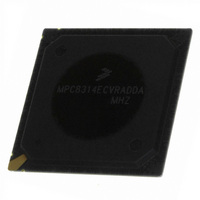
MPC8314ECVRADDA Freescale Semiconductor, MPC8314ECVRADDA Datasheet - Page 101

MPC8314ECVRADDA
Manufacturer Part Number
MPC8314ECVRADDA
Description
MPU POWERQUICC II PRO 620-PBGA
Manufacturer
Freescale Semiconductor
Datasheet
1.MPC8314VRADDA.pdf
(106 pages)
Specifications of MPC8314ECVRADDA
Processor Type
MPC83xx PowerQUICC II Pro 32-Bit
Speed
266MHz
Voltage
1V
Mounting Type
Surface Mount
Package / Case
620-PBGA
Processor Series
MPC8xxx
Core
e300
Data Bus Width
32 bit
Maximum Clock Frequency
50 MHz
Maximum Operating Temperature
+ 105 C
Mounting Style
SMD/SMT
Minimum Operating Temperature
- 40 C
Lead Free Status / RoHS Status
Lead free / RoHS Compliant
Features
-
Lead Free Status / Rohs Status
Lead free / RoHS Compliant
Available stocks
Company
Part Number
Manufacturer
Quantity
Price
Company:
Part Number:
MPC8314ECVRADDA
Manufacturer:
Freescale Semiconductor
Quantity:
135
Company:
Part Number:
MPC8314ECVRADDA
Manufacturer:
Freescale Semiconductor
Quantity:
10 000
lift the edge of the package or peel the package from the board. Such peeling forces reduce the solder joint
lifetime of the package. Recommended maximum force on the top of the package is 10 lb force (45
Newtons). If an adhesive attachment is planned, the adhesive should be intended for attachment to painted
or plastic surfaces and its performance verified under the application requirements.
24.3.1
When heat sink is used, the junction temperature is determined from a thermocouple inserted at the
interface between the case of the package and the interface material. A clearance slot or hole is normally
required in the heat sink. Minimizing the size of the clearance is important to minimize the change in
thermal performance caused by removing part of the thermal interface to the heat sink temperature and
then back calculate the case temperature using a separate measurement of the thermal resistance of the
interface. From this case temperature, the junction temperature is determined from the junction to case
thermal resistance.
25 System Design Information
This section provides electrical and thermal design recommendations for successful application of the
MPC8314E.
25.1
The MPC8314E includes two PLLs.
25.2
Each of the PLLs listed above is provided with power through independent power supply pins
(AVDD1,AVDD2 respectively). The AV
these voltages are derived directly from VDD through a low frequency filter scheme such as the following.
Freescale Semiconductor
1. The platform PLL (AVDD2) generates the platform clock from the externally supplied
2. The e300 Core PLL (AVDD1
SYS_CLKIN input. The frequency ratio between the platform and SYS_CLKIN is selected using
the platform PLL ratio configuration bits as described in
Configuration.”
frequency ratio between the e300 core clock and the platform clock is selected using the e300
PLL ratio configuration bits as described in
System Clocking
PLL Power Supply Filtering
Experimental Determination of the Junction Temperature with a
Heat Sink
Where
MPC8314E PowerQUICC
T
T
R
P
D
J
C
θ
JC
= T
is the case temperature of the package
is the power dissipation
is the junction-to-case thermal resistance
C
+ (R
θ
)
JC
generates the core clock as a slave to the platform clock. The
DD
x P
™
II Pro Processor Hardware Specifications, Rev. 0
D
level should always be equivalent to VDD, and preferably
)
Section 23.2, “Core PLL Configuration.”
Section 23.1, “System PLL
System Design Information
101


