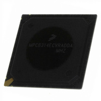
MPC8314ECVRADDA Freescale Semiconductor, MPC8314ECVRADDA Datasheet - Page 16

MPC8314ECVRADDA
Manufacturer Part Number
MPC8314ECVRADDA
Description
MPU POWERQUICC II PRO 620-PBGA
Manufacturer
Freescale Semiconductor
Datasheet
1.MPC8314VRADDA.pdf
(106 pages)
Specifications of MPC8314ECVRADDA
Processor Type
MPC83xx PowerQUICC II Pro 32-Bit
Speed
266MHz
Voltage
1V
Mounting Type
Surface Mount
Package / Case
620-PBGA
Processor Series
MPC8xxx
Core
e300
Data Bus Width
32 bit
Maximum Clock Frequency
50 MHz
Maximum Operating Temperature
+ 105 C
Mounting Style
SMD/SMT
Minimum Operating Temperature
- 40 C
Lead Free Status / RoHS Status
Lead free / RoHS Compliant
Features
-
Lead Free Status / Rohs Status
Lead free / RoHS Compliant
Available stocks
Company
Part Number
Manufacturer
Quantity
Price
Company:
Part Number:
MPC8314ECVRADDA
Manufacturer:
Freescale Semiconductor
Quantity:
135
Company:
Part Number:
MPC8314ECVRADDA
Manufacturer:
Freescale Semiconductor
Quantity:
10 000
DDR and DDR2 SDRAM
Time for the device to turn on POR config signals with respect to the negation of
HRESET
Notes:
1. t
2. t
3. POR configuration signals consists of CFG_RESET_SOURCE[0:3] and CFG_SYS_CLKIN_DIV.
Table 10
7
This section describes the DC and AC electrical specifications for the DDR SDRAM interface of the
MPC8314E. Note that DDR SDRAM is GVDD(typ) = 2.5 V and DDR2 SDRAM is GVDD(typ) = 1.8 V.
7.1 DDR and DDR2 SDRAM DC Electrical Characteristics
Table 11
MPC8314E when GVDD(typ) = 1.8 V
16
I/O supply voltage
I/O reference voltage
I/O termination voltage
Input high voltage
Input low voltage
Output leakage current
Output high current (V
GVDD= 1.7V)
clock is applied to the SYS_CLKIN input, and PCI_SYNC_IN period depends on the value of CFG_SYS_CLKIN_DIV.
PCI_SYNC_IN
SYS_CLKIN
DDR and DDR2 SDRAM
Parameter/Condition
provides the recommended operating conditions for the DDR2 SDRAM component(s) of the
provides the PLL lock times.
is the clock period of the input clock applied to SYS_CLKIN. It is only valid when the device is in PCI host mode.
System PLL lock times
e300 core PLL lock times
SerDes (SGMII/PCIExp Phy) PLL lock times
USB phy PLL lock times
is the clock period of the input clock applied to PCI_SYNC_IN. When the device is In PCI host mode the primary
Table 11. DDR2 SDRAM DC Electrical Characteristics for GVDD(typ) = 1.8 V
OUT
MPC8314E PowerQUICC
Table 9. RESET Initialization Timing Specifications (continued)
= 1.420 V,
Parameter/Condition
Symbol
MVREF
GVDD
.
V
I
V
V
I
OZ
OH
Table 10. PLL Lock Times
TT
IH
IL
™
II Pro Processor Hardware Specifications, Rev. 0
MVREF+ 0.125
MVREF – 0.04
0.49 × GVDD
–13.4
–0.3
–9.9
Min
1.7
Min
—
—
—
—
Max
100
100
100
100
MVREF – 0.125
MVREF + 0.04
0.51 × GVDD
1
GVDD + 0.3
Max
1.9
9.9
—
Unit
—
μs
μs
μs
μs
Freescale Semiconductor
t
PCI_SYNC_IN
Notes
—
—
—
—
Unit
mA
μA
V
V
V
V
V
Notes
—
—
—
4
1, 3
1
2
3


