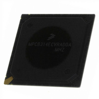
MPC8314ECVRADDA Freescale Semiconductor, MPC8314ECVRADDA Datasheet - Page 4

MPC8314ECVRADDA
Manufacturer Part Number
MPC8314ECVRADDA
Description
MPU POWERQUICC II PRO 620-PBGA
Manufacturer
Freescale Semiconductor
Datasheet
1.MPC8314VRADDA.pdf
(106 pages)
Specifications of MPC8314ECVRADDA
Processor Type
MPC83xx PowerQUICC II Pro 32-Bit
Speed
266MHz
Voltage
1V
Mounting Type
Surface Mount
Package / Case
620-PBGA
Processor Series
MPC8xxx
Core
e300
Data Bus Width
32 bit
Maximum Clock Frequency
50 MHz
Maximum Operating Temperature
+ 105 C
Mounting Style
SMD/SMT
Minimum Operating Temperature
- 40 C
Lead Free Status / RoHS Status
Lead free / RoHS Compliant
Features
-
Lead Free Status / Rohs Status
Lead free / RoHS Compliant
Available stocks
Company
Part Number
Manufacturer
Quantity
Price
Company:
Part Number:
MPC8314ECVRADDA
Manufacturer:
Freescale Semiconductor
Quantity:
135
Company:
Part Number:
MPC8314ECVRADDA
Manufacturer:
Freescale Semiconductor
Quantity:
10 000
MPC8314E Features
2.4
The DDR1/DDR2 memory controller includes the following features:
2.5
The PCI controller includes the following features:
2.6
The TDM interface includes the following features:
4
•
•
•
•
•
•
•
•
•
•
•
•
•
•
•
•
•
•
•
•
•
•
•
— Implements CRC32C as required for iSCSI header and payload checksums, CRC32 as required
Single 16- or 32-bit interface supporting both DDR1 and DDR2 SDRAM
Support for up to 266 MHz data rate
Support for two physical banks (chip selects), each bank independently addressable
64-Mbit to 2-Gbit (for DDR1) and to 4-Gbit (for DDR2) devices with x8/x16 data ports (no direct
x4 support)
Support for one 16-bit device or two 8-bit devices on a 16-bit bus or two 16-bit devices on a 32-bit
bus
Support for up to 16 simultaneous open pages
Supports auto refresh
On-the-fly power management using CKE
1.8-/2.5-V SSTL2 compatible I/O
Designed to comply with PCI Local Bus Specification Revision 2.3
Single 32-bit data PCI interface operates at up to 66 MHz
PCI 3.3-V compatible (not 5-V compatible)
Support for host and agent modes
On-chip arbitration, supporting three external masters on PCI
Selectable hardware-enforced coherency
Independent receive and transmit with dedicated data, clock and frame sync line
Separate or shared RCK and TCK whose source can be either internal or external
Glueless interface to E1/T1 frames and MVIP, SCAS, and H.110 buses
Up to 128 time slots, where each slot can be programmed to be active or inactive
8- or 16-bit word widths
The TDM Transmitter Sync Signal (TFS), Transmitter Clock Signal (TCK) and Receiver Clock
Signal (RCK) can be configured as either input or output
Frame sync and data signals can be programmed to be sampled either on the rising edge or on the
falling edge of the clock
DDR Memory Controller
PCI Controller
TDM Interface
for IEEE 802 packets, as well as for programmable 32 bit CRC polynomials
MPC8314E PowerQUICC
™
II Pro Processor Hardware Specifications, Rev. 0
Freescale Semiconductor


