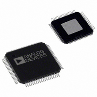
AD9852ASVZ Analog Devices Inc, AD9852ASVZ Datasheet - Page 24

AD9852ASVZ
Manufacturer Part Number
AD9852ASVZ
Description
IC DDS SYNTHESIZER CMOS 80-TQFP
Manufacturer
Analog Devices Inc
Datasheet
1.AD9852ASTZ.pdf
(52 pages)
Specifications of AD9852ASVZ
Resolution (bits)
12 b
Master Fclk
300MHz
Tuning Word Width (bits)
48 b
Voltage - Supply
3.14 V ~ 3.47 V
Operating Temperature
-40°C ~ 85°C
Mounting Type
Surface Mount
Package / Case
80-TQFP Exposed Pad, 80-eTQFP, 80-HTQFP, 80-VQFP
Transmitting Current
815mA
Rf Ic Case Style
TQFP
No. Of Pins
80
Supply Voltage Range
3.135V To 3.465V
Operating Temperature Range
-40°C To +85°C
Msl
MSL 3 - 168 Hours
Frequency Max
300MHz
Lead Free Status / RoHS Status
Lead free / RoHS Compliant
For Use With
AD9852/PCBZ - BOARD EVAL FOR AD9852
Lead Free Status / Rohs Status
Compliant
Available stocks
Company
Part Number
Manufacturer
Quantity
Price
Company:
Part Number:
AD9852ASVZ
Manufacturer:
ADI
Quantity:
263
Company:
Part Number:
AD9852ASVZ
Manufacturer:
Analog Devices Inc
Quantity:
10 000
Part Number:
AD9852ASVZ
Manufacturer:
ADI/亚德诺
Quantity:
20 000
AD9852
supplied or internally generated. See the Internal and External
Update Clock section for a discussion of the I/O update.
Alternatively, the CLR ACC2 control bit (Register Address 1F hex)
is available to clear both the frequency accumulator (ACC1)
and the phase accumulator (ACC2). When this bit is set high,
the output of the phase accumulator results in 0 Hz output from
the DDS. As long as this bit is set high, the frequency and phase
accumulators are cleared, resulting in 0 Hz output. To return to
the previous DDS operation, CLR ACC2 must be set to logic
low. This bit is useful for generating pulsed FM.
Figure 43 graphically illustrates the effect of the CLR ACC2 bit on
the DDS output frequency. Reprogramming the registers while
the CLR ACC2 bit is high allows a new FTW1 frequency and
slope to be loaded.
RAMP RATE
I/O UD CLK
CLR ACC1
MODE
FTW1
DFW
FREQUENCY
000 (DEFAULT)
F1
0
0
Figure 42. Effect of CLR ACC1 in FM Chirp Mode
Rev. E | Page 24 of 52
DELTA FREQUENCY WORD
RAMP RATE
011 (CHIRP)
Another function only available in the chirp mode is the
HOLD pin (Pin 29). This function stops the clock signal to the
ramp rate counter, thereby halting any further clocking pulses
to the frequency accumulator, ACC1.
The effect is to halt the chirp at the frequency existing just
before the HOLD pin is pulled high. When the HOLD pin is
returned low, the clock resumes and chirp continues. During a
hold condition, the user can change the programming registers;
however, the ramp rate counter must resume operation at its
previous rate until a count of 0 is obtained before a new ramp
rate count can be loaded. Figure 44 illustrates the effect of the
hold function on the DDS output frequency.
F1


