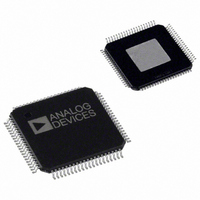
AD9852ASVZ Analog Devices Inc, AD9852ASVZ Datasheet - Page 29

AD9852ASVZ
Manufacturer Part Number
AD9852ASVZ
Description
IC DDS SYNTHESIZER CMOS 80-TQFP
Manufacturer
Analog Devices Inc
Datasheet
1.AD9852ASTZ.pdf
(52 pages)
Specifications of AD9852ASVZ
Resolution (bits)
12 b
Master Fclk
300MHz
Tuning Word Width (bits)
48 b
Voltage - Supply
3.14 V ~ 3.47 V
Operating Temperature
-40°C ~ 85°C
Mounting Type
Surface Mount
Package / Case
80-TQFP Exposed Pad, 80-eTQFP, 80-HTQFP, 80-VQFP
Transmitting Current
815mA
Rf Ic Case Style
TQFP
No. Of Pins
80
Supply Voltage Range
3.135V To 3.465V
Operating Temperature Range
-40°C To +85°C
Msl
MSL 3 - 168 Hours
Frequency Max
300MHz
Lead Free Status / RoHS Status
Lead free / RoHS Compliant
For Use With
AD9852/PCBZ - BOARD EVAL FOR AD9852
Lead Free Status / Rohs Status
Compliant
Available stocks
Company
Part Number
Manufacturer
Quantity
Price
Company:
Part Number:
AD9852ASVZ
Manufacturer:
ADI
Quantity:
263
Company:
Part Number:
AD9852ASVZ
Manufacturer:
Analog Devices Inc
Quantity:
10 000
Part Number:
AD9852ASVZ
Manufacturer:
ADI/亚德诺
Quantity:
20 000
COSINE DAC
The cosine output of the DDS drives the cosine DAC (300 MSPS
maximum). Its maximum output amplitude is set by the DAC R
resistor at Pin 56. This is a current-output DAC with a full-scale
maximum output of 20 mA; however, a nominal 10 mA output
current provides best spurious-free dynamic range (SFDR) perfor-
mance. The value of R
amps. DAC output compliance specifications limit the maximum
voltage developed at the outputs to −0.5 V to +1 V. Voltages
developed beyond this limitation cause excessive DAC distortion
and possibly permanent damage. The user must choose a proper
load impedance to limit the output voltage swing to the compliance
limits. Both DAC outputs should be terminated equally for best
SFDR, especially at higher output frequencies, where harmonic
distortion errors are more prominent.
The cosine DAC is preceded by an inverse sin(x)/x filter
(also called an inverse sinc filter) that precompensates for
DAC output amplitude variations over frequency to achieve
flat amplitude response from dc to Nyquist. This DAC can be
powered down when not needed by setting the DAC PD bit
high (Address 1D hex of the control register). Cosine DAC
outputs are designated as IOUT1 (Pin 48) and IOUT1 (Pin 49).
CONTROL DAC
The control DAC output can provide dc control levels to
external circuitry, generate ac signals, or enable duty cycle
control of the on-board comparator. The input to the control
DAC is configured to accept twos complement data supplied by
the user. Data is channeled through the serial or parallel inter-
face to the 12-bit control DAC register (Address 26 hex and
Address 27 hex) at a maximum data rate of 100 MHz. This DAC
is clocked at the system clock, 300 MSPS (maximum), and has
the same maximum output current capability as that of the
cosine DAC. The single R
full-scale output current for both DACs. When not needed, the
control DAC can be powered down separately to conserve power
by setting the control DAC power-down bit high (Address 1D hex).
Control DAC outputs are designated as IOUT2 (Pin 52) and
IOUT2 (Pin 51).
SET
is 39.93/I
SET
resistor on the AD9852 sets the
OUT
, where I
OUT
is expressed in
Rev. E | Page 29 of 52
SET
INVERSE SINC FUNCTION
This filter precompensates input data to the cosine DAC for
the sin(x)/x roll-off characteristic inherent in the DAC’s
output spectrum. This allows wide bandwidth signals, such
as QPSK, to be output from the DAC without appreciable
amplitude variations as a function of frequency. The inverse
sinc function can be bypassed to significantly reduce power
consumption, especially at higher clock speeds.
Inverse sinc is engaged by default and is bypassed by bringing
the bypass inverse sinc bit high in Control Register 20 hex, as
noted in Table 9.
REFCLK MULTIPLIER
The REFCLK multiplier is a programmable PLL-based
reference clock multiplier that allows the user to select an
integer clock multiplying value over the range of 4× to 20×. Use
of this function allows users to input as little as 15 MHz at the
REFCLK input to produce a 300 MHz internal system clock.
Five bits in Control Register 1E hex set the multiplier value, as
described in Table 8.
The REFCLK multiplier function can be bypassed to allow
direct clocking of the AD9852 from an external clock source.
The system clock for the AD9852 is either the output of the
REFCLK multiplier (if it is engaged) or the REFCLK inputs.
REFCLK can be either a single-ended or differential input by
setting Pin 64 (DIFF CLK ENABLE) low or high, respectively.
PLL Range Bit
The PLL range bit selects the frequency range of the REFCLK
multiplier PLL. For operation from 200 MHz to 300 MHz
(internal system clock rate), the PLL range bit should be set to
Logic 1. For operation below 200 MHz, set the PLL range bit to
Logic 0. The PLL range bit adjusts the PLL loop parameters for
optimized phase noise performance within each range.
–0.5
–1.0
–1.5
–2.0
–2.5
–3.0
–3.5
–4.0
4.0
3.5
3.0
2.5
2.0
1.5
1.0
0.5
0
0
FREQUENCY NORMALIZED TO SAMPLE RATE
Figure 48. Inverse Sinc Filter Response
0.1
0.2
0.3
SYSTEM
SINC
ISF
0.4
AD9852
0.5


