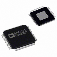
AD9852ASVZ Analog Devices Inc, AD9852ASVZ Datasheet - Page 31

AD9852ASVZ
Manufacturer Part Number
AD9852ASVZ
Description
IC DDS SYNTHESIZER CMOS 80-TQFP
Manufacturer
Analog Devices Inc
Datasheet
1.AD9852ASTZ.pdf
(52 pages)
Specifications of AD9852ASVZ
Resolution (bits)
12 b
Master Fclk
300MHz
Tuning Word Width (bits)
48 b
Voltage - Supply
3.14 V ~ 3.47 V
Operating Temperature
-40°C ~ 85°C
Mounting Type
Surface Mount
Package / Case
80-TQFP Exposed Pad, 80-eTQFP, 80-HTQFP, 80-VQFP
Transmitting Current
815mA
Rf Ic Case Style
TQFP
No. Of Pins
80
Supply Voltage Range
3.135V To 3.465V
Operating Temperature Range
-40°C To +85°C
Msl
MSL 3 - 168 Hours
Frequency Max
300MHz
Lead Free Status / RoHS Status
Lead free / RoHS Compliant
For Use With
AD9852/PCBZ - BOARD EVAL FOR AD9852
Lead Free Status / Rohs Status
Compliant
Available stocks
Company
Part Number
Manufacturer
Quantity
Price
Company:
Part Number:
AD9852ASVZ
Manufacturer:
ADI
Quantity:
263
Company:
Part Number:
AD9852ASVZ
Manufacturer:
Analog Devices Inc
Quantity:
10 000
Part Number:
AD9852ASVZ
Manufacturer:
ADI/亚德诺
Quantity:
20 000
PROGRAMMING THE AD9852
The AD9852 Register Layout table (Table 9) contains information
for programming a chip for a desired functionality. Although
many applications require very little programming to configure
the AD9852, some use all 12 accessible register banks. The
AD9852 supports an 8-bit parallel I/O operation or an SPI-
compatible serial I/O operation. All accessible registers can be
written and read back in either I/O operating mode.
S/P SELECT (Pin 70) is used to configure the I/O mode.
Systems that use a parallel I/O mode must connect the S/P
SELECT pin to V
must tie the S/P SELECT pin to GND.
Regardless of the mode, the I/O port data is written to a buffer
memory that only affects operation of the part after the contents
of the buffer memory are transferred to the register banks. This
transfer of information occurs synchronous to the system clock
in one of two ways:
•
•
MASTER RESET
The MASTER RESET pin must be held at logic high active for
a minimum of 10 system clock cycles. This initializes the com-
munication bus and loads the default values listed in Table 9.
PARALLEL I/O OPERATION
With the S/P SELECT pin tied high, the parallel I/O mode is
active. The I/O port is compatible with industry-standard DSPs
and microcontrollers. Six address bits, eight bidirectional data
bits, and separate write/read control inputs comprise the I/O
port pins.
Parallel I/O operation allows write access to each byte of any
register in a single I/O operation of up to one per 10.5 ns.
Readback capability for each register is included to ease
designing with the AD9852.
Reads are not guaranteed at 100 MHz, because they are
intended for software debugging only.
Parallel I/O operation timing diagrams are shown in Figure 49
and Figure 50.
The transfer is internally controlled at a rate programmed
by the user.
The transfer is externally controlled by the user. I/O opera-
tions can occur in the absence of REFCLK, but data cannot be
moved from the buffer memory to the register bank without
REFCLK. (See the Internal and External Update Clock
section for details.)
DD
. Systems that operate in the serial I/O mode
Rev. E | Page 31 of 52
Table 8. REFCLK Multiplier Control Register Values
Multiplier Value
4
5
6
7
8
9
10
11
12
13
14
15
16
17
18
19
20
SERIAL PORT I/O OPERATION
With the S/P SELECT pin tied low, the serial I/O mode is
active. The AD9852 serial port is a flexible, synchronous, serial
communication port, allowing easy interface to many industry-
standard microcontrollers and microprocessors. The serial I/O
is compatible with most synchronous transfer formats, including
both the Motorola 6905/11 SPI and Intel 8051 SSR protocols.
The interface allows read/write access to all 12 registers that
configure the AD9852 and can be configured as a single-pin
I/O (SDIO) or two unidirectional pins for input and output
(SDIO/SDO). Data transfers are supported in MSB- or LSB-
first format at up to 10 MHz.
When configured for serial I/O operation, most pins from the
AD9852 parallel port are inactive; only some pins are used for
serial I/O operation. Table 10 describes pin requirements for
serial I/O operation.
When operating the device in the serial I/O mode, it is best to
use the external I/O update clock mode to avoid an I/O update
clock occurring during a serial communication cycle. Such an
occurrence may cause incorrect programming due to a partial
data transfer. Therefore, users should write to the device between
I/O update clocks. To exit the default internal update mode,
program the device for external update operation at power-up
before starting the REFCLK signal but after a master reset.
Starting the REFCLK causes this information to transfer to the
register bank, forcing the device to switch to external update mode.
Bit 4
0
0
0
0
0
0
0
0
0
0
0
0
1
1
1
1
1
Bit 3
0
0
0
0
1
1
1
1
1
1
1
1
0
0
0
0
0
Reference Multiplier
Bit 2
1
1
1
1
0
0
0
0
1
1
1
1
0
0
0
0
1
Bit 1
0
0
1
1
0
0
1
1
0
0
1
1
0
0
1
1
0
AD9852
Bit 0
0
1
0
1
0
1
0
1
0
1
0
1
0
1
0
1
0


