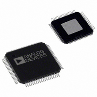
AD9852ASVZ Analog Devices Inc, AD9852ASVZ Datasheet - Page 28

AD9852ASVZ
Manufacturer Part Number
AD9852ASVZ
Description
IC DDS SYNTHESIZER CMOS 80-TQFP
Manufacturer
Analog Devices Inc
Datasheet
1.AD9852ASTZ.pdf
(52 pages)
Specifications of AD9852ASVZ
Resolution (bits)
12 b
Master Fclk
300MHz
Tuning Word Width (bits)
48 b
Voltage - Supply
3.14 V ~ 3.47 V
Operating Temperature
-40°C ~ 85°C
Mounting Type
Surface Mount
Package / Case
80-TQFP Exposed Pad, 80-eTQFP, 80-HTQFP, 80-VQFP
Transmitting Current
815mA
Rf Ic Case Style
TQFP
No. Of Pins
80
Supply Voltage Range
3.135V To 3.465V
Operating Temperature Range
-40°C To +85°C
Msl
MSL 3 - 168 Hours
Frequency Max
300MHz
Lead Free Status / RoHS Status
Lead free / RoHS Compliant
For Use With
AD9852/PCBZ - BOARD EVAL FOR AD9852
Lead Free Status / Rohs Status
Compliant
Available stocks
Company
Part Number
Manufacturer
Quantity
Price
Company:
Part Number:
AD9852ASVZ
Manufacturer:
ADI
Quantity:
263
Company:
Part Number:
AD9852ASVZ
Manufacturer:
Analog Devices Inc
Quantity:
10 000
Part Number:
AD9852ASVZ
Manufacturer:
ADI/亚德诺
Quantity:
20 000
AD9852
The two fixed elements of the transition time are the period of
the system clock (which drives the ramp rate counter) and the
number of amplitude steps (4096). For example, if the system
clock of the AD9852 is 100 MHz (10 ns period) and the ramp
rate counter is programmed for a minimum count of 3, two system
clock periods are required: one rising edge loads the countdown
value, and the next edge decrements the counter from 3 to 2. If the
countdown value is less than 3, the ramp rate counter stalls and
therefore produces a constant scaling value to the digital multiplier.
This stall condition may have an application for the user.
The relationship of the 8-bit countdown value to the time between
output pulses is given as
where N is the 8-bit countdown value.
(N + 1) × System Clock Period
Figure 47. Block Diagram of the Digital Multiplier Section Responsible for the Output Shaped Keying Function
DDS DIGITAL
OUTPUT
USER-PROGRAMMABLE
SIGNAL IN
DIGITAL
KEYING MULTIPLIER
12-BIT MULTIPLIER
OUTPUT SHAPED
REGISTER
12
OSK EN = 0
OSK EN = 1
12
Rev. E | Page 28 of 52
(BYPASS MULTIPLIER)
OSK INT = 0
12-BIT DIGITAL
MULTIPLIER
12
COUNTER
UP/DOWN
OSK INT = 1
A total of 4096 output pulses is required to advance the 12-bit
up-counter from zero scale to full scale. Therefore, the minimum
output shaped keying ramp time for a 100 MHz system clock is
The maximum ramp time is
Finally, by changing the logic state of Pin 30, output shaped
keying automatically performs the programmed output envelope
functions when OSK INT is high. A logic high on Pin 30 causes
the outputs to linearly ramp up to full-scale amplitude and hold
until the logic level is changed to low, causing the outputs to
ramp down to zero scale.
12-BIT
12
4096 × 4 × 10 ns ≈ 164 μs
4096 × 256 × 10 ns ≈ 10.5 ms
ON/OFF OUTPUT SHAPED
KEYING PIN
OSK EN = 0
OSK EN = 1
1
8-BIT RAMP
COUNTER
RATE
12
COSINE
DAC
SYSTEM
CLOCK


