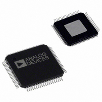
AD9852ASVZ Analog Devices Inc, AD9852ASVZ Datasheet - Page 25

AD9852ASVZ
Manufacturer Part Number
AD9852ASVZ
Description
IC DDS SYNTHESIZER CMOS 80-TQFP
Manufacturer
Analog Devices Inc
Datasheet
1.AD9852ASTZ.pdf
(52 pages)
Specifications of AD9852ASVZ
Resolution (bits)
12 b
Master Fclk
300MHz
Tuning Word Width (bits)
48 b
Voltage - Supply
3.14 V ~ 3.47 V
Operating Temperature
-40°C ~ 85°C
Mounting Type
Surface Mount
Package / Case
80-TQFP Exposed Pad, 80-eTQFP, 80-HTQFP, 80-VQFP
Transmitting Current
815mA
Rf Ic Case Style
TQFP
No. Of Pins
80
Supply Voltage Range
3.135V To 3.465V
Operating Temperature Range
-40°C To +85°C
Msl
MSL 3 - 168 Hours
Frequency Max
300MHz
Lead Free Status / RoHS Status
Lead free / RoHS Compliant
For Use With
AD9852/PCBZ - BOARD EVAL FOR AD9852
Lead Free Status / Rohs Status
Compliant
Available stocks
Company
Part Number
Manufacturer
Quantity
Price
Company:
Part Number:
AD9852ASVZ
Manufacturer:
ADI
Quantity:
263
Company:
Part Number:
AD9852ASVZ
Manufacturer:
Analog Devices Inc
Quantity:
10 000
Part Number:
AD9852ASVZ
Manufacturer:
ADI/亚德诺
Quantity:
20 000
The 32-bit automatic I/O update counter can be used to
construct complex chirp or ramped FSK sequences. Because
this internal counter is synchronized with the AD9852 system
clock, it allows precisely timed program changes to be invoked.
For such changes, the user need only reprogram the desired
registers before the automatic I/O update clock is generated.
In chirp mode, the destination frequency is not directly speci-
fied. If the user fails to control the chirp, the DDS automatically
confines itself to the frequency range between dc and Nyquist.
Unless terminated by the user, the chirp continues until power
is removed.
RAMP RATE
RAMP RATE
I/O UD CLK
I/O UD CLK
CLR ACC2
MODE
MODE
HOLD
DPW
TW1
DFW
TW1
FREQUENCY
FREQUENCY
000 (DEFAULT)
000 (DEFAULT)
F1
F1
0
0
0
0
Figure 43. Effect of CLR ACC2 in FM Chirp Mode
Figure 44. Example of Hold Function
Rev. E | Page 25 of 52
DELTA FREQUENCY WORD
RAMP RATE
011 (CHIRP)
When the chirp destination frequency is reached, the user can
choose any of the following actions:
•
•
•
011 (CHIRP)
F1
Stop at the destination frequency either by using the
HOLD pin or by loading all 0s into the delta frequency
word registers of the frequency accumulator (ACC1).
Use the HOLD pin function to stop the chirp, and then ramp
down the output amplitude either by using the digital multi-
plier stages and the output shaped keying pin (Pin 30) or by
using the program register control (Address 21 hex to
Address 24 hex).
Abruptly end the transmission with the CLR ACC2 bit.
AD9852


