DK-DEV-2AGX260N Altera, DK-DEV-2AGX260N Datasheet - Page 16
DK-DEV-2AGX260N
Manufacturer Part Number
DK-DEV-2AGX260N
Description
KIT DEV FPGA 2AGX260 W/6.375G TX
Manufacturer
Altera
Series
Arria II GXr
Type
FPGAr
Specifications of DK-DEV-2AGX260N
Contents
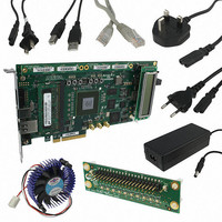
Board, Cables, CD, DVD, Power Supply
Silicon Manufacturer
Altera
Core Architecture
FPGA
Core Sub-architecture
Arria
Silicon Core Number
EP2
Silicon Family Name
Arria II GX
Rohs Compliant
Yes
For Use With/related Products
EP2AGX260
Lead Free Status / RoHS Status
Lead free / RoHS Compliant
Other names
544-2696
Available stocks
Company
Part Number
Manufacturer
Quantity
Price
Company:

Part Number:
DK-DEV-2AGX260N
Manufacturer:
Altera
Quantity:
135


4–2
Factory Default Switch Settings
Table 4–1. SW3 Dip Switch Settings
Arria II GX FPGA Development Kit, 6G Edition User Guide
1
2
3
4
Switch
PCIe MODE
PCIe MODE
PCIe MODE
PCIe MODE
Board
Label
This section shows the factory switch settings for the Arria II GX FPGA development
board, 6G edition.
each switch on the top side of the board.
Figure 4–1. Switch Locations and Default Settings on the Board Top
To restore the switches to their factory default settings, perform the following steps:
1. Set DIP switch bank (SW3) to match
J9
JTAG Control
Switch 1 has the following options:
■
■
Switch 2 has the following options:
■
■
Switch 3 has the following options:
■
■
Switch 4 has the following options:
■
■
Jumpers
When on, the PCIe card PRSNT2_x1 signal is connected to PCIe card
PRSNT1 signal.
When off, the PCIe card PRSNT2_x1 signal floats.
When on, the PCIe card PRSNT2_x4 signal is connected to PCIe card
PRSNT1 signal.
When off, the PCIe card PRSNT2_x4 signal floats.
When on, the PCIe card PRSNT2_x8 signal is connected to PCIe card
PRSNT1 signal.
When off, the PCIe card PRSNT2_x8 signal floats.
When on, the switch is ignored. It is not connected.
When off, the switch is ignored. It is not connected.
Figure 4–1
shows the switch locations and the default position of
PCIe MODE
DIP Switch
Function
ON
SW3
1
DIP Switch
2
3
ON
User
1
SW2
Table 4–1
4
2
3
4
ON = 0
OFF = 1
and
Figure
Board Settings
Chapter 4: Development Board Setup
DIP Switch
ON
1 2 3 4 5 6 7 8
4–1.
SW4
Factory Default Switch Settings
July 2010 Altera Corporation
ON = 0
OFF = 1
Position
Default
Off
On
On
On
Related parts for DK-DEV-2AGX260N
Image
Part Number
Description
Manufacturer
Datasheet
Request
R

Part Number:
Description:
KIT DEV ARRIA II GX FPGA 2AGX125
Manufacturer:
Altera
Datasheet:

Part Number:
Description:
KIT DEV CYCLONE III LS EP3CLS200
Manufacturer:
Altera
Datasheet:

Part Number:
Description:
KIT DEV STRATIX IV FPGA 4SE530
Manufacturer:
Altera
Datasheet:

Part Number:
Description:
KIT DEV MAX V 5M570Z
Manufacturer:
Altera
Datasheet:

Part Number:
Description:
KIT DEV STRATIX V FPGA 5SGXEA7
Manufacturer:
Altera
Datasheet:

Part Number:
Description:
KIT DEVELOPMENT STRATIX III
Manufacturer:
Altera
Datasheet:

Part Number:
Description:
KIT DEVELOPMENT STRATIX IV
Manufacturer:
Altera
Datasheet:

Part Number:
Description:
KIT DEV ARRIA GX 1AGX60N
Manufacturer:
Altera
Datasheet:
Part Number:
Description:
KIT STARTER CYCLONE IV GX
Manufacturer:
Altera
Datasheet:
Part Number:
Description:
KIT DEVELOPMENT STRATIX IV
Manufacturer:
Altera
Datasheet:

Part Number:
Description:
CPLD, EP610 Family, ECMOS Process, 300 Gates, 16 Macro Cells, 16 Reg., 16 User I/Os, 5V Supply, 35 Speed Grade, 24DIP
Manufacturer:
Altera Corporation
Datasheet:
Part Number:
Description:
CPLD, EP610 Family, ECMOS Process, 300 Gates, 16 Macro Cells, 16 Reg., 16 User I/Os, 5V Supply, 15 Speed Grade, 24DIP
Manufacturer:
Altera Corporation
Datasheet: