DK-DEV-2AGX260N Altera, DK-DEV-2AGX260N Datasheet - Page 23
DK-DEV-2AGX260N
Manufacturer Part Number
DK-DEV-2AGX260N
Description
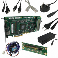
KIT DEV FPGA 2AGX260 W/6.375G TX
Manufacturer
Altera
Series
Arria II GXr
Type
FPGAr
Specifications of DK-DEV-2AGX260N
Contents
Board, Cables, CD, DVD, Power Supply
Silicon Manufacturer
Altera
Core Architecture
FPGA
Core Sub-architecture
Arria
Silicon Core Number
EP2
Silicon Family Name
Arria II GX
Rohs Compliant
Yes
For Use With/related Products
EP2AGX260
Lead Free Status / RoHS Status
Lead free / RoHS Compliant
Other names
544-2696
Available stocks
Company
Part Number
Manufacturer
Quantity
Price
Company:

Part Number:
DK-DEV-2AGX260N
Manufacturer:
Altera
Quantity:
135


Chapter 6: Board Test System
Preparing the Board
Preparing the Board
Running the Board Test System
July 2010 Altera Corporation
1
1
The Board Test System and Power Monitor share the JTAG bus with other
applications like the Nios II debugger and the SignalTap
Analyzer. Because the Quartus II programmer uses most of the bandwidth of the
JTAG bus, other applications using the JTAG bus might time out. Be sure to close the
other applications before attempting to reconfigure the FPGA using the Quartus II
Programmer.
With the power to the board off, perform the following steps:
1. Connect the USB cable to the board.
2. Verify the settings for the board settings DIP switch bank (SW4) match
3. Set the USR LOAD switch (SW4.4) to the on position.
4. Verify the settings for the JTAG jumper block (J9) match
5. Turn the power to the board on. The board loads the design stored in the user
To run the application, navigate to the <install
dir>\kits\arriaIIGX_2agx260_fpga\examples\board_test_system directory and run
the BoardTestSystem.exe application.
On Windows, click Start > All Programs > Altera > Arria II GX FPGA Development
Kit, 6G Edition <version> > Board Test System to run the application.
A GUI appears, displaying the application tab that corresponds to the design running
in the FPGA. The Arria II GX FPGA development board, 6G edition’s flash memory
ships preconfigured with the design that corresponds to the Config, GPIO, and
SRAM&Flash tabs.
on page
These settings determine the devices to include in the JTAG chain.
f
hardware 1 portion of flash memory into the FPGA. If your board is still in the
factory configuration or if you have downloaded a newer version of the Board Test
System to flash memory through the Board Update Portal, the design that loads
tests accessing the GPIO, SRAM, and flash memory.
c
For more information about the board’s DIP switch and jumper settings,
refer to the
Manual.
To ensure operating stability, keep the USB cable connected and the board
powered on when running the demonstration application. The application
cannot run correctly unless the USB cable is attached and the board is on.
4–3.
Arria II GX FPGA Development Board, 6G Edition Reference
Arria II GX FPGA Development Kit, 6G Edition User Guide
®
II Embedded Logic
Table 4–3 on page
Table 4–2
4–3.
6–3
Related parts for DK-DEV-2AGX260N
Image
Part Number
Description
Manufacturer
Datasheet
Request
R

Part Number:
Description:
KIT DEV ARRIA II GX FPGA 2AGX125
Manufacturer:
Altera
Datasheet:

Part Number:
Description:
KIT DEV CYCLONE III LS EP3CLS200
Manufacturer:
Altera
Datasheet:

Part Number:
Description:
KIT DEV STRATIX IV FPGA 4SE530
Manufacturer:
Altera
Datasheet:

Part Number:
Description:
KIT DEV MAX V 5M570Z
Manufacturer:
Altera
Datasheet:

Part Number:
Description:
KIT DEV STRATIX V FPGA 5SGXEA7
Manufacturer:
Altera
Datasheet:

Part Number:
Description:
KIT DEVELOPMENT STRATIX III
Manufacturer:
Altera
Datasheet:

Part Number:
Description:
KIT DEVELOPMENT STRATIX IV
Manufacturer:
Altera
Datasheet:

Part Number:
Description:
KIT DEV ARRIA GX 1AGX60N
Manufacturer:
Altera
Datasheet:
Part Number:
Description:
KIT STARTER CYCLONE IV GX
Manufacturer:
Altera
Datasheet:
Part Number:
Description:
KIT DEVELOPMENT STRATIX IV
Manufacturer:
Altera
Datasheet:

Part Number:
Description:
CPLD, EP610 Family, ECMOS Process, 300 Gates, 16 Macro Cells, 16 Reg., 16 User I/Os, 5V Supply, 35 Speed Grade, 24DIP
Manufacturer:
Altera Corporation
Datasheet:
Part Number:
Description:
CPLD, EP610 Family, ECMOS Process, 300 Gates, 16 Macro Cells, 16 Reg., 16 User I/Os, 5V Supply, 15 Speed Grade, 24DIP
Manufacturer:
Altera Corporation
Datasheet: