DK-DEV-2AGX260N Altera, DK-DEV-2AGX260N Datasheet - Page 25
DK-DEV-2AGX260N
Manufacturer Part Number
DK-DEV-2AGX260N
Description
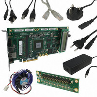
KIT DEV FPGA 2AGX260 W/6.375G TX
Manufacturer
Altera
Series
Arria II GXr
Type
FPGAr
Specifications of DK-DEV-2AGX260N
Contents
Board, Cables, CD, DVD, Power Supply
Silicon Manufacturer
Altera
Core Architecture
FPGA
Core Sub-architecture
Arria
Silicon Core Number
EP2
Silicon Family Name
Arria II GX
Rohs Compliant
Yes
For Use With/related Products
EP2AGX260
Lead Free Status / RoHS Status
Lead free / RoHS Compliant
Other names
544-2696
Available stocks
Company
Part Number
Manufacturer
Quantity
Price
Company:

Part Number:
DK-DEV-2AGX260N
Manufacturer:
Altera
Quantity:
135


Chapter 6: Board Test System
Using the Board Test System
July 2010 Altera Corporation
■
■
MAX II Registers
The MAX II registers control allow you to view and change the current MAX II
register values as described in
take effect immediately. For example, selecting a new frequency in the OCR1 list
immediately changes the clock frequency on the board.
Table 6–1. MAX II Registers
System Reset
(SRST)
Page Select Register
(PSR)
Page Select Override
(PSO)
Page Select Switch
(PSS)
Oscillator Control
Register 1 (OCR1)
Oscillator Control
Register 2 (OCR2)
MAX II ver—Indicates the version of MAX II code currently running on the board.
The MAX II code resides in the <install
dir>\kits\arriaIIGX_2agx260_fpga\examples directory. Newer revisions of this
code might be available on the
page of the Altera website.
MAC—Indicates the MAC address of the board.
Register Name
Write only
Read / Write
Read / Write
Read only
Read / Write
Read / Write
Read/Write
Capability
Table
Set to 0 to initiate an FPGA reconfiguration.
Determines which of the up to eight (0-7) pages of flash
memory to use for FPGA reconfiguration. The flash memory
ships with pages 0 and 1 preconfigured.
When set to 0, the value in PSR determines the page of
flash memory to use for FPGA reconfiguration. When set to
1, the value in PSS determines the page of flash memory to
use for FPGA reconfiguration.
Holds the current value of the iluminated CONFIG LED (D11-
D13) based on the following encoding:
■
■
■
Determines the U26 oscillator output frequency based on
the following options:
■
■
■
■
Determines the U30 oscillator output frequency based on
the following options:
■
■
■
■
You cannot change OCR2 from the GUI.
Arria II GX FPGA Development Kit, 6G Edition
6–1. Changes to the register values with the GUI
0 = CONFIG LED (D13)and corresponds to the flash
memory page for the factory hardware design
1 = CONFIG LED (D12)and corresponds to the flash
memory page for the user hardware 1 design
2 = CONFIG LED (D11)and corresponds to the flash
memory page for the user hardware 2 design
0 = 100 MHz
1 = 125 MHz
2 = 150 MHz
3 = 156.25 MHz
0 = 100 MHz
1 = 125 MHz
2 = 150 MHz
3 = 156.25 MHz
Arria II GX FPGA Development Kit, 6G Edition User Guide
Description
6–5
Related parts for DK-DEV-2AGX260N
Image
Part Number
Description
Manufacturer
Datasheet
Request
R

Part Number:
Description:
KIT DEV ARRIA II GX FPGA 2AGX125
Manufacturer:
Altera
Datasheet:

Part Number:
Description:
KIT DEV CYCLONE III LS EP3CLS200
Manufacturer:
Altera
Datasheet:

Part Number:
Description:
KIT DEV STRATIX IV FPGA 4SE530
Manufacturer:
Altera
Datasheet:

Part Number:
Description:
KIT DEV MAX V 5M570Z
Manufacturer:
Altera
Datasheet:

Part Number:
Description:
KIT DEV STRATIX V FPGA 5SGXEA7
Manufacturer:
Altera
Datasheet:

Part Number:
Description:
KIT DEVELOPMENT STRATIX III
Manufacturer:
Altera
Datasheet:

Part Number:
Description:
KIT DEVELOPMENT STRATIX IV
Manufacturer:
Altera
Datasheet:

Part Number:
Description:
KIT DEV ARRIA GX 1AGX60N
Manufacturer:
Altera
Datasheet:
Part Number:
Description:
KIT STARTER CYCLONE IV GX
Manufacturer:
Altera
Datasheet:
Part Number:
Description:
KIT DEVELOPMENT STRATIX IV
Manufacturer:
Altera
Datasheet:

Part Number:
Description:
CPLD, EP610 Family, ECMOS Process, 300 Gates, 16 Macro Cells, 16 Reg., 16 User I/Os, 5V Supply, 35 Speed Grade, 24DIP
Manufacturer:
Altera Corporation
Datasheet:
Part Number:
Description:
CPLD, EP610 Family, ECMOS Process, 300 Gates, 16 Macro Cells, 16 Reg., 16 User I/Os, 5V Supply, 15 Speed Grade, 24DIP
Manufacturer:
Altera Corporation
Datasheet: