DK-DEV-2AGX260N Altera, DK-DEV-2AGX260N Datasheet - Page 41
DK-DEV-2AGX260N
Manufacturer Part Number
DK-DEV-2AGX260N
Description
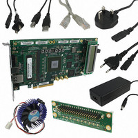
KIT DEV FPGA 2AGX260 W/6.375G TX
Manufacturer
Altera
Series
Arria II GXr
Type
FPGAr
Specifications of DK-DEV-2AGX260N
Contents
Board, Cables, CD, DVD, Power Supply
Silicon Manufacturer
Altera
Core Architecture
FPGA
Core Sub-architecture
Arria
Silicon Core Number
EP2
Silicon Family Name
Arria II GX
Rohs Compliant
Yes
For Use With/related Products
EP2AGX260
Lead Free Status / RoHS Status
Lead free / RoHS Compliant
Other names
544-2696
Available stocks
Company
Part Number
Manufacturer
Quantity
Price
Company:

Part Number:
DK-DEV-2AGX260N
Manufacturer:
Altera
Quantity:
135


Introduction
CFI Flash Memory Map
July 2010 Altera Corporation
f
As you develop your own project using the Altera tools, you can program the flash
memory device so that your own design loads from flash memory into the FPGA on
power up. This appendix describes the preprogrammed contents of the common flash
interface (CFI) flash memory device on the Arria II GX FPGA development board, 6G
edition and the Nios II EDS tools involved with reprogramming the user portions of
the flash memory device.
The Arria II GX FPGA development board, 6G edition ships with the CFI flash device
preprogrammed with a default factory FPGA configuration for running the Board
Update Portal design example and a default user configuration for running the Board
Test System demonstration. There are several other factory software files written to
the CFI flash device to support the Board Update Portal. These software files were
created using the Nios II EDS, just as the hardware design was created using the
Quartus II software.
For more information about Altera development tools, refer to the
page of the Altera website.
Table A–1
flash device. For the Board Update Portal to run correctly and update designs in the
user memory, this memory map must not be altered.
Table A–1. Byte Address Flash Memory Map
Unused
Unused
Unused
Unused
User software
Factory software
zipfs (html, web content)
User hardware 2
User hardware 1
Factory hardware
PFL option bits
Board information
Ethernet option bits
User design reset vector
Block Description
shows the default memory contents of the 512-Mb (64-MB) single-die CFI
A. Programming the Flash Memory
32 KB
32 KB
32 KB
32 KB
16,384 KB
8,1092 KB
8,192 KB
10,880 KB
10,880 KB
10,880 KB
32 KB
32 KB
32 KB
32 KB
Size
0x03FF8000 - 0x03FFFFFF
0x03FF0000 - 0x03FF7FFF
0x03FE8000 - 0x03FEFFFF
0x03FE0000 - 0x03FE7FFF
0x0300.0000 - 0x03FDFFFF
0x02800000 - 0x02FFFFFF
0x02000000 - 0x027FFFFF
0x01560000 - 0x01FFFFFF
0x00AC0000 - 0x0155FFFF
0x00020000 - 0x00ABFFFF
0x00018000 - 0x0001FFFF
0x00010000 - 0x00017FFF
0x00008000 - 0x0000FFFF
0x00000000 - 0x00007FFF
Arria II GX FPGA Development Kit, 6G Edition User Guide
Address Range
Design Software
Device
Related parts for DK-DEV-2AGX260N
Image
Part Number
Description
Manufacturer
Datasheet
Request
R

Part Number:
Description:
KIT DEV ARRIA II GX FPGA 2AGX125
Manufacturer:
Altera
Datasheet:

Part Number:
Description:
KIT DEV CYCLONE III LS EP3CLS200
Manufacturer:
Altera
Datasheet:

Part Number:
Description:
KIT DEV STRATIX IV FPGA 4SE530
Manufacturer:
Altera
Datasheet:

Part Number:
Description:
KIT DEV MAX V 5M570Z
Manufacturer:
Altera
Datasheet:

Part Number:
Description:
KIT DEV STRATIX V FPGA 5SGXEA7
Manufacturer:
Altera
Datasheet:

Part Number:
Description:
KIT DEVELOPMENT STRATIX III
Manufacturer:
Altera
Datasheet:

Part Number:
Description:
KIT DEVELOPMENT STRATIX IV
Manufacturer:
Altera
Datasheet:

Part Number:
Description:
KIT DEV ARRIA GX 1AGX60N
Manufacturer:
Altera
Datasheet:
Part Number:
Description:
KIT STARTER CYCLONE IV GX
Manufacturer:
Altera
Datasheet:
Part Number:
Description:
KIT DEVELOPMENT STRATIX IV
Manufacturer:
Altera
Datasheet:

Part Number:
Description:
CPLD, EP610 Family, ECMOS Process, 300 Gates, 16 Macro Cells, 16 Reg., 16 User I/Os, 5V Supply, 35 Speed Grade, 24DIP
Manufacturer:
Altera Corporation
Datasheet:
Part Number:
Description:
CPLD, EP610 Family, ECMOS Process, 300 Gates, 16 Macro Cells, 16 Reg., 16 User I/Os, 5V Supply, 15 Speed Grade, 24DIP
Manufacturer:
Altera Corporation
Datasheet: