DK-DEV-2AGX260N Altera, DK-DEV-2AGX260N Datasheet - Page 26
DK-DEV-2AGX260N
Manufacturer Part Number
DK-DEV-2AGX260N
Description
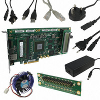
KIT DEV FPGA 2AGX260 W/6.375G TX
Manufacturer
Altera
Series
Arria II GXr
Type
FPGAr
Specifications of DK-DEV-2AGX260N
Contents
Board, Cables, CD, DVD, Power Supply
Silicon Manufacturer
Altera
Core Architecture
FPGA
Core Sub-architecture
Arria
Silicon Core Number
EP2
Silicon Family Name
Arria II GX
Rohs Compliant
Yes
For Use With/related Products
EP2AGX260
Lead Free Status / RoHS Status
Lead free / RoHS Compliant
Other names
544-2696
Available stocks
Company
Part Number
Manufacturer
Quantity
Price
Company:

Part Number:
DK-DEV-2AGX260N
Manufacturer:
Altera
Quantity:
135


6–6
Arria II GX FPGA Development Kit, 6G Edition User Guide
1
1
■
■
■
■
■
Because the Config tab requires that a specific design is running in the FPGA at a
specific clock speed, writing a 0 to SRST; writing a 1, 2, or 3 to OCR2; or changing the
PSO value can cause the Board Test System to stop running.
JTAG Chain Devices
The JTAG chain devices control shows all the devices currently in the JTAG chain.
The Arria II GX device is always the first device in the chain.
Uninstalling the shunt jumper from jumper J9 pins 1-2 includes the MAX II device in
the JTAG chain.
Flash Memory Map
The Flash memory map control shows the memory map of the flash memory device
on your board.
PSO—Sets the MAX II PSO register. The following options are available:
■
■
PSR—Sets the MAX II PSR register. The numerical values in the list corresponds to
the page of flash memory to load during FPGA reconfiguration. Refer to
for more information.
PSS—Displays the MAX II PSS register value. Refer to
available options.
OCR1—Sets the MAX II OCR1 register. Refer to
options.
SRST—Resets the system and reloads the FPGA with a design from flash memory
based on the other MAX II register values. Refer to
Use PSR—Allows the PSR to determine the page of flash memory to use for
FPGA reconfiguration.
Use PSS—Allows the PSS to determine the page of flash memory to use for
FPGA reconfiguration.
Table 6–1
Table 6–1
Table 6–1
for the list of available
Chapter 6: Board Test System
July 2010 Altera Corporation
for more information.
Using the Board Test System
for the list of
Table 6–1
Related parts for DK-DEV-2AGX260N
Image
Part Number
Description
Manufacturer
Datasheet
Request
R

Part Number:
Description:
KIT DEV ARRIA II GX FPGA 2AGX125
Manufacturer:
Altera
Datasheet:

Part Number:
Description:
KIT DEV CYCLONE III LS EP3CLS200
Manufacturer:
Altera
Datasheet:

Part Number:
Description:
KIT DEV STRATIX IV FPGA 4SE530
Manufacturer:
Altera
Datasheet:

Part Number:
Description:
KIT DEV MAX V 5M570Z
Manufacturer:
Altera
Datasheet:

Part Number:
Description:
KIT DEV STRATIX V FPGA 5SGXEA7
Manufacturer:
Altera
Datasheet:

Part Number:
Description:
KIT DEVELOPMENT STRATIX III
Manufacturer:
Altera
Datasheet:

Part Number:
Description:
KIT DEVELOPMENT STRATIX IV
Manufacturer:
Altera
Datasheet:

Part Number:
Description:
KIT DEV ARRIA GX 1AGX60N
Manufacturer:
Altera
Datasheet:
Part Number:
Description:
KIT STARTER CYCLONE IV GX
Manufacturer:
Altera
Datasheet:
Part Number:
Description:
KIT DEVELOPMENT STRATIX IV
Manufacturer:
Altera
Datasheet:

Part Number:
Description:
CPLD, EP610 Family, ECMOS Process, 300 Gates, 16 Macro Cells, 16 Reg., 16 User I/Os, 5V Supply, 35 Speed Grade, 24DIP
Manufacturer:
Altera Corporation
Datasheet:
Part Number:
Description:
CPLD, EP610 Family, ECMOS Process, 300 Gates, 16 Macro Cells, 16 Reg., 16 User I/Os, 5V Supply, 15 Speed Grade, 24DIP
Manufacturer:
Altera Corporation
Datasheet: