DK-DEV-2AGX260N Altera, DK-DEV-2AGX260N Datasheet - Page 44
DK-DEV-2AGX260N
Manufacturer Part Number
DK-DEV-2AGX260N
Description
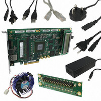
KIT DEV FPGA 2AGX260 W/6.375G TX
Manufacturer
Altera
Series
Arria II GXr
Type
FPGAr
Specifications of DK-DEV-2AGX260N
Contents
Board, Cables, CD, DVD, Power Supply
Silicon Manufacturer
Altera
Core Architecture
FPGA
Core Sub-architecture
Arria
Silicon Core Number
EP2
Silicon Family Name
Arria II GX
Rohs Compliant
Yes
For Use With/related Products
EP2AGX260
Lead Free Status / RoHS Status
Lead free / RoHS Compliant
Other names
544-2696
Available stocks
Company
Part Number
Manufacturer
Quantity
Price
Company:

Part Number:
DK-DEV-2AGX260N
Manufacturer:
Altera
Quantity:
135


A–4
Restoring the Flash Device to the Factory Settings
Arria II GX FPGA Development Kit, 6G Edition User Guide
f
11. Set the USR LOAD switch (SW4.4) to the on position and power cycle the board, or
Programming the board is now complete.
For more information about the nios2-flash-programmer utility, refer to the
Flash Programmer User
This section describes how to restore the original factory contents to the flash memory
device on the FPGA development board, 6G edition. Make sure you have the Nios II
EDS installed, and perform the following instructions:
1. Set the board switches to the factory default settings described in
2. Launch the Quartus II Programmer to configure the FPGA with a .sof capable of
3. Click Add File and select <install
4. Turn on the Program/Configure option for the added file.
5. Click Start to download the selected configuration file to the FPGA. Configuration
6. On the Windows Start menu, click All Programs > Altera > Nios II EDS > Nios II
7. In the Nios II command shell, navigate to the <install
8. After all flash programming completes, cycle the POWER switch (SW1) off then
9. Using the Quartus II Programmer, click Add File and select <install
10. Turn on the Program/Configure option for the added file.
11. Click Start to download the selected configuration file to the FPGA. Configuration
press the IMAGE SEL button (PB6) until the CONFIG1 LED (D12) illuminates and
then press the LOAD IMAGE button (PB5) to load and run the user hardware 1
design. Refer to
Switch Settings” on page
flash programming. Refer to
Programmer” on page 6–19
dir>\kits\arriaIIGX_2agx260_fpga\factory_recovery\ArriaIIGX_2agx260_dev_
bup.sof.
is complete when the progress bar reaches 100%. The CONF DONE LED (D14)
and the four user LEDs (D7-D10) illuminate indicating that the flash device is
ready for programming.
Command Shell.
dir>\kits\arriaIIGX_2agx260_fpga\factory_recovery directory and type the
following command to run the restore script:
./restore.sh r
Restoring the flash memory might take several minutes. Follow any instructions
that appear in the Nios II command shell.
on.
dir>\kits\arriaIIGX_2agx260_fpga\factory_recovery\ArriaIIGX_2agx260_dev_
bup.sof.
is complete when the progress bar reaches 100%. The CONF DONE LED (D14)
and the four user LEDs (D7-D10) illuminate indicating the flash memory device is
now restored with the factory contents.
Table 6–1 on page 6–5
Guide.
4–2.
for more information.
“Configuring the FPGA Using the Quartus II
for information about the CONFIG LEDs.
Restoring the Flash Device to the Factory Settings
July 2010 Altera Corporation
“Factory Default
Nios II
Chapter :
Related parts for DK-DEV-2AGX260N
Image
Part Number
Description
Manufacturer
Datasheet
Request
R

Part Number:
Description:
KIT DEV ARRIA II GX FPGA 2AGX125
Manufacturer:
Altera
Datasheet:

Part Number:
Description:
KIT DEV CYCLONE III LS EP3CLS200
Manufacturer:
Altera
Datasheet:

Part Number:
Description:
KIT DEV STRATIX IV FPGA 4SE530
Manufacturer:
Altera
Datasheet:

Part Number:
Description:
KIT DEV MAX V 5M570Z
Manufacturer:
Altera
Datasheet:

Part Number:
Description:
KIT DEV STRATIX V FPGA 5SGXEA7
Manufacturer:
Altera
Datasheet:

Part Number:
Description:
KIT DEVELOPMENT STRATIX III
Manufacturer:
Altera
Datasheet:

Part Number:
Description:
KIT DEVELOPMENT STRATIX IV
Manufacturer:
Altera
Datasheet:

Part Number:
Description:
KIT DEV ARRIA GX 1AGX60N
Manufacturer:
Altera
Datasheet:
Part Number:
Description:
KIT STARTER CYCLONE IV GX
Manufacturer:
Altera
Datasheet:
Part Number:
Description:
KIT DEVELOPMENT STRATIX IV
Manufacturer:
Altera
Datasheet:

Part Number:
Description:
CPLD, EP610 Family, ECMOS Process, 300 Gates, 16 Macro Cells, 16 Reg., 16 User I/Os, 5V Supply, 35 Speed Grade, 24DIP
Manufacturer:
Altera Corporation
Datasheet:
Part Number:
Description:
CPLD, EP610 Family, ECMOS Process, 300 Gates, 16 Macro Cells, 16 Reg., 16 User I/Os, 5V Supply, 15 Speed Grade, 24DIP
Manufacturer:
Altera Corporation
Datasheet: