HW-V5-ML506-UNI-G Xilinx Inc, HW-V5-ML506-UNI-G Datasheet - Page 18
HW-V5-ML506-UNI-G
Manufacturer Part Number
HW-V5-ML506-UNI-G
Description
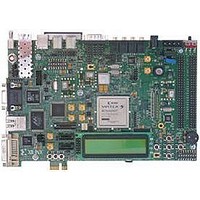
EVALUATION PLATFORM VIRTEX-5
Manufacturer
Xilinx Inc
Series
Virtex™-5 SXTr
Type
DSPr
Datasheet
1.HW-V5-ML507-UNI-G.pdf
(60 pages)
Specifications of HW-V5-ML506-UNI-G
Contents
Evaluation Platform, DVI Adapter and CompactFlash Card
Silicon Manufacturer
Xilinx
Features
JTAG Programming Interface, Platform Flash, External Clocking
Kit Contents
Board, Cable, PSU, CD, Docs
Silicon Family Name
Virtex-5
Silicon Core Number
XC5VSX50TFFG1136
Rohs Compliant
Yes
Lead Free Status / RoHS Status
Lead free / RoHS Compliant
For Use With/related Products
XC5VSX50TFFG1136
Lead Free Status / RoHS Status
Lead free / RoHS Compliant, Lead free / RoHS Compliant
Available stocks
Company
Part Number
Manufacturer
Quantity
Price


Chapter 1: ML505/ML506/ML507 Evaluation Platform
18
2. DDR2 SODIMM
Digitally Controlled Impedance
MIG Compliance
Some FPGA banks can support the digitally controlled impedance (DCI) feature in
Virtex-5 FPGAs. Support for DCI is summarized in
Table 1-2: DCI Capability of FPGA Bank
The ML50x platform is shipped with a single-rank unregistered 256 MB SODIMM. The
DDR2 SODIMM used is generally a Micron MT4HTF3264HY-53E or similar module. Serial
Presence Detect (SPD) using an IIC interface to the DDR DIMM is also supported with the
FPGA.
Note:
rates might be possible but are not tested.
The ML50x DDR2 interface is MIG pinout compliant. The MIG DDR2 routing guidelines
outlined in the Xilinx Memory Interface Generator (MIG) User Guide
achieved.
The board’s DDR2 SODIMM memory interface is designed to the requirements defined by
the MIG User Guide using the MIG tool. The MIG documentation requires that designers
follow the MIG pinout and layout guidelines. The MIG tool generates and ensures that the
proper FPGA I/O pin selections are made in support of the board’s DDR2 interface. The
initial pin selection for the board was modified and then re-verified to meet the MIG
pinout requirements. To ensure a robust interface, the ML50x DDR2 layout incorporates
matched trace lengths for data signals to the corresponding data strobe signal as defined in
the MIG user guide. See
about MIG and Virtex-5 FPGAs in general.
FPGA Bank
The board is only tested for DDR2 SDRAM operation at a 400 MHz data rate. Faster data
11
12
13
14
15
16
17
18
21
1
2
3
4
Not supported
Not supported
Not supported
Not supported
Yes, 49.9Ω resistors are installed
Not supported
Yes, 49.9Ω resistors are installed
Yes, 49.9Ω resistors are installed
Yes, 49.9Ω resistors are installed
Yes, 49.9Ω resistors are installed
Yes, 49.9Ω resistors are installed
Not supported
Yes, 49.9Ω resistors are installed
Appendix C, “References”
www.xilinx.com
DCI Capability
ML505/ML506/ML507 Evaluation Platform
Table
for links to additional information
1-2.
UG347 (v3.1.1) October 7, 2009
[Ref 17]
have been
R
Related parts for HW-V5-ML506-UNI-G
Image
Part Number
Description
Manufacturer
Datasheet
Request
R

Part Number:
Description:
IC CPLD .8K 36MCELL 44-VQFP
Manufacturer:
Xilinx Inc
Datasheet:

Part Number:
Description:
IC CPLD 72MCRCELL 10NS 44VQFP
Manufacturer:
Xilinx Inc
Datasheet:

Part Number:
Description:
IC CPLD 1.6K 72MCELL 64-VQFP
Manufacturer:
Xilinx Inc
Datasheet:

Part Number:
Description:
IC CR-II CPLD 64MCELL 44-VQFP
Manufacturer:
Xilinx Inc
Datasheet:

Part Number:
Description:
IC CPLD 1.6K 72MCELL 100-TQFP
Manufacturer:
Xilinx Inc
Datasheet:

Part Number:
Description:
IC CR-II CPLD 64MCELL 56-BGA
Manufacturer:
Xilinx Inc
Datasheet:

Part Number:
Description:
IC CPLD 72MCRCELL 7.5NS 44VQFP
Manufacturer:
Xilinx Inc
Datasheet:
Part Number:
Description:
IC CR-II CPLD 64MCELL 100-VQFP
Manufacturer:
Xilinx Inc
Datasheet:
Part Number:
Description:
IC CPLD 1.6K 72MCELL 100-TQFP
Manufacturer:
Xilinx Inc
Datasheet:

Part Number:
Description:
IC CPLD 72MCRCELL 7.5NS 64VQFP
Manufacturer:
Xilinx Inc
Datasheet:
Part Number:
Description:
IC CPLD 1.6K 72MCELL 100-TQFP
Manufacturer:
Xilinx Inc
Datasheet:

Part Number:
Description:
IC CPLD 1.5K 64MCELL HP 44-VQFP
Manufacturer:
Xilinx Inc

Part Number:
Description:
IC CPLD 36MCRCELL 15NS 44PLCC
Manufacturer:
Xilinx Inc
Datasheet:

Part Number:
Description:
IC CPLD 36MCRCELL 10NS 44PLCC
Manufacturer:
Xilinx Inc
Datasheet:

Part Number:
Description:
IC CPLD 1.5K 64MCELL HP 44-VQFP
Manufacturer:
Xilinx Inc