HW-V5-ML506-UNI-G Xilinx Inc, HW-V5-ML506-UNI-G Datasheet - Page 20
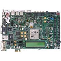
HW-V5-ML506-UNI-G
Manufacturer Part Number
HW-V5-ML506-UNI-G
Description
EVALUATION PLATFORM VIRTEX-5
Manufacturer
Xilinx Inc
Series
Virtex™-5 SXTr
Type
DSPr
Datasheet
1.HW-V5-ML507-UNI-G.pdf
(60 pages)
Specifications of HW-V5-ML506-UNI-G
Contents
Evaluation Platform, DVI Adapter and CompactFlash Card
Silicon Manufacturer
Xilinx
Features
JTAG Programming Interface, Platform Flash, External Clocking
Kit Contents
Board, Cable, PSU, CD, Docs
Silicon Family Name
Virtex-5
Silicon Core Number
XC5VSX50TFFG1136
Rohs Compliant
Yes
Lead Free Status / RoHS Status
Lead free / RoHS Compliant
For Use With/related Products
XC5VSX50TFFG1136
Lead Free Status / RoHS Status
Lead free / RoHS Compliant, Lead free / RoHS Compliant
Available stocks
Company
Part Number
Manufacturer
Quantity
Price


Chapter 1: ML505/ML506/ML507 Evaluation Platform
20
5. LCD Brightness and Contrast Adjustment
6. GPIO DIP Switches (Active-High)
FPGA. The programmable clock generator provides the following factory default single-
ended outputs:
•
•
•
•
•
If users change the factory default configuration of the clock generator chip, the related
reference design material might not work as designed. Instructions for returning the
IDT5V9885 to the factory default configuration are provided in
“Programming the IDT Clock Chip.”
Table 1-4: Oscillator Socket Connections
Turning potentiometer R87 adjusts the image contrast of the character LCD. The
potentiometer should be turned with a screwdriver.
Eight general-purpose (active-High) DIP switches are connected to the user I/O pins of the
FPGA.
Table 1-5: DIP Switch Connections (SW4)
Designator
Reference
GPIO_DIP_SW1
GPIO_DIP_SW2
GPIO_DIP_SW3
GPIO_DIP_SW4
GPIO_DIP_SW5
GPIO_DIP_SW6
GPIO_DIP_SW7
GPIO_DIP_SW8
25 MHz to the Ethernet PHY (U16)
14 MHz to the audio codec (U22)
27 MHz to the USB Controller (U23)
33 MHz to the Xilinx System ACE CF (U2)
33 MHz, 27 MHz, and a differential 200 MHz clock to the Xilinx FPGA
U8
U8
U8
U8
X1
Table 1-5
SW4
CLK_33MHZ_FPGA
CLK_27MHZ_FPGA
summarizes these connections.
CLK_FPGA_N
CLK_FPGA_P
Clock Name
USER_CLK
www.xilinx.com
FPGA Pin
AG27
AC25
AC24
AF25
AF26
AE27
AE26
U25
FPGA Pin
AH15
AH17
AG18
K19
L19
ML505/ML506/ML507 Evaluation Platform
100 MHz single-ended
33 MHz single-ended
27 MHz single-ended
200 MHz differential pair (pos)
200 MHz differential pair (neg)
UG347 (v3.1.1) October 7, 2009
Description
Appendix B,
R
Related parts for HW-V5-ML506-UNI-G
Image
Part Number
Description
Manufacturer
Datasheet
Request
R

Part Number:
Description:
IC CPLD .8K 36MCELL 44-VQFP
Manufacturer:
Xilinx Inc
Datasheet:

Part Number:
Description:
IC CPLD 72MCRCELL 10NS 44VQFP
Manufacturer:
Xilinx Inc
Datasheet:

Part Number:
Description:
IC CPLD 1.6K 72MCELL 64-VQFP
Manufacturer:
Xilinx Inc
Datasheet:

Part Number:
Description:
IC CR-II CPLD 64MCELL 44-VQFP
Manufacturer:
Xilinx Inc
Datasheet:

Part Number:
Description:
IC CPLD 1.6K 72MCELL 100-TQFP
Manufacturer:
Xilinx Inc
Datasheet:

Part Number:
Description:
IC CR-II CPLD 64MCELL 56-BGA
Manufacturer:
Xilinx Inc
Datasheet:

Part Number:
Description:
IC CPLD 72MCRCELL 7.5NS 44VQFP
Manufacturer:
Xilinx Inc
Datasheet:
Part Number:
Description:
IC CR-II CPLD 64MCELL 100-VQFP
Manufacturer:
Xilinx Inc
Datasheet:
Part Number:
Description:
IC CPLD 1.6K 72MCELL 100-TQFP
Manufacturer:
Xilinx Inc
Datasheet:

Part Number:
Description:
IC CPLD 72MCRCELL 7.5NS 64VQFP
Manufacturer:
Xilinx Inc
Datasheet:
Part Number:
Description:
IC CPLD 1.6K 72MCELL 100-TQFP
Manufacturer:
Xilinx Inc
Datasheet:

Part Number:
Description:
IC CPLD 1.5K 64MCELL HP 44-VQFP
Manufacturer:
Xilinx Inc

Part Number:
Description:
IC CPLD 36MCRCELL 15NS 44PLCC
Manufacturer:
Xilinx Inc
Datasheet:

Part Number:
Description:
IC CPLD 36MCRCELL 10NS 44PLCC
Manufacturer:
Xilinx Inc
Datasheet:

Part Number:
Description:
IC CPLD 1.5K 64MCELL HP 44-VQFP
Manufacturer:
Xilinx Inc