HW-V5-ML506-UNI-G Xilinx Inc, HW-V5-ML506-UNI-G Datasheet - Page 47
HW-V5-ML506-UNI-G
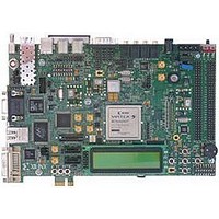
Manufacturer Part Number
HW-V5-ML506-UNI-G
Description
EVALUATION PLATFORM VIRTEX-5
Manufacturer
Xilinx Inc
Series
Virtex™-5 SXTr
Type
DSPr
Datasheet
1.HW-V5-ML507-UNI-G.pdf
(60 pages)
Specifications of HW-V5-ML506-UNI-G
Contents
Evaluation Platform, DVI Adapter and CompactFlash Card
Silicon Manufacturer
Xilinx
Features
JTAG Programming Interface, Platform Flash, External Clocking
Kit Contents
Board, Cable, PSU, CD, Docs
Silicon Family Name
Virtex-5
Silicon Core Number
XC5VSX50TFFG1136
Rohs Compliant
Yes
Lead Free Status / RoHS Status
Lead free / RoHS Compliant
For Use With/related Products
XC5VSX50TFFG1136
Lead Free Status / RoHS Status
Lead free / RoHS Compliant, Lead free / RoHS Compliant
Available stocks
Company
Part Number
Manufacturer
Quantity
Price


Table 1-31: Configurations for Clock Source and Frequency Options
ML505/ML506/ML507 Evaluation Platform
UG347 (v3.1.1) October 7, 2009
Notes:
1. Factory default setting.
2. A 1 equates to the DIP switch in the on position.
3. For Fibre Channel support, see
N0
1
0
0
1
0
1
1
1
0
1
N1
1
1
0
0
0
1
0
1
1
1
DIP Switch SW6 [1:8] Value
N2
0
1
0
0
1
1
1
0
1
0
R
M0
0
0
0
0
1
1
0
0
0
1
SATA GTP/GTX Transceiver Clock Generation
SGMII / Loopback GTP/GTX Transceiver Clock Generation
M1
0
0
0
0
1
1
1
1
1
1
The native output of the ICS843001-21 is LVPECL, so a resistor network is present to
change the voltage swing to LVDS levels. The LVDS output is then multiplexed out
through Series AC coupling capacitors to allow the clock input of the FPGA to set the
common mode voltage.
An Integrated Circuit Systems ICS844051-1 chip generates a high-quality, low-jitter,
75-MHz or 150-MHz LVDS clock from an inexpensive 25-MHz crystal oscillator. This clock
is sent to the GTP/GTX transceiver driving the SATA connectors. Jumper J56 sets the
SATA GTP/GTX transceiver clock frequency (see
capacitors are also present to allow the clock input of the FPGA to set the common mode
voltage.
Table 1-32: Configuration for SATA GTP/GTX Clock Signals
An Integrated Circuit Systems ICS844021I chip generates a high-quality, low-jitter,
125-MHz LVDS clock from an inexpensive 25-MHz crystal oscillator. This clock is sent to
the GTPs driving the SGMII or onboard loopback interfaces. Series AC coupling capacitors
are also present to allow the clock input of the FPGA to set the common mode voltage.
SATA Clock Frequency
M2 SEL1 SEL0
1
1
1
1
0
0
0
0
0
0
Answer Record
SATA Clock Signal
0
0
0
0
1
1
1
1
1
1
1
1
1
1
0
0
0
0
0
0
Input Ref
Clock
(MHz)
24918.
19.44
19.44
19.44
19.44
25
25
25
25
25
25
www.xilinx.com
M Divider
Value
Jumper J56
• Jumper Off = 75 MHz
• Jumper On = 150 MHz
32
32
32
32
25
25
24
24
24
25
Board Connection
N Divider
Value
10
4
8
1
2
5
6
4
8
4
(MHz)
622.08
622.08
622.08
622.08
V
625
625
600
600
600
625
Table
CO
1-32). Series AC coupling
Frequency
Output
155.52
622.08
156.25
(MHz)
311.04
150
77.76
62.5
125
100
75
(1)
Detailed Description
Gigabit Ethernet
Gigabit Ethernet
Application
XAUI/SRIO
PCI Express
SONET
SONET
SONET
SONET
SATA
SATA
47
Related parts for HW-V5-ML506-UNI-G
Image
Part Number
Description
Manufacturer
Datasheet
Request
R

Part Number:
Description:
IC CPLD .8K 36MCELL 44-VQFP
Manufacturer:
Xilinx Inc
Datasheet:

Part Number:
Description:
IC CPLD 72MCRCELL 10NS 44VQFP
Manufacturer:
Xilinx Inc
Datasheet:

Part Number:
Description:
IC CPLD 1.6K 72MCELL 64-VQFP
Manufacturer:
Xilinx Inc
Datasheet:

Part Number:
Description:
IC CR-II CPLD 64MCELL 44-VQFP
Manufacturer:
Xilinx Inc
Datasheet:

Part Number:
Description:
IC CPLD 1.6K 72MCELL 100-TQFP
Manufacturer:
Xilinx Inc
Datasheet:

Part Number:
Description:
IC CR-II CPLD 64MCELL 56-BGA
Manufacturer:
Xilinx Inc
Datasheet:

Part Number:
Description:
IC CPLD 72MCRCELL 7.5NS 44VQFP
Manufacturer:
Xilinx Inc
Datasheet:
Part Number:
Description:
IC CR-II CPLD 64MCELL 100-VQFP
Manufacturer:
Xilinx Inc
Datasheet:
Part Number:
Description:
IC CPLD 1.6K 72MCELL 100-TQFP
Manufacturer:
Xilinx Inc
Datasheet:

Part Number:
Description:
IC CPLD 72MCRCELL 7.5NS 64VQFP
Manufacturer:
Xilinx Inc
Datasheet:
Part Number:
Description:
IC CPLD 1.6K 72MCELL 100-TQFP
Manufacturer:
Xilinx Inc
Datasheet:

Part Number:
Description:
IC CPLD 1.5K 64MCELL HP 44-VQFP
Manufacturer:
Xilinx Inc

Part Number:
Description:
IC CPLD 36MCRCELL 15NS 44PLCC
Manufacturer:
Xilinx Inc
Datasheet:

Part Number:
Description:
IC CPLD 36MCRCELL 10NS 44PLCC
Manufacturer:
Xilinx Inc
Datasheet:

Part Number:
Description:
IC CPLD 1.5K 64MCELL HP 44-VQFP
Manufacturer:
Xilinx Inc