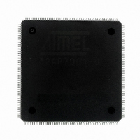
AT32AP7001-ALUT Atmel, AT32AP7001-ALUT Datasheet - Page 537

AT32AP7001-ALUT
Manufacturer Part Number
AT32AP7001-ALUT
Description
IC MCU 32BIT AVR32 208-LQFP
Manufacturer
Atmel
Series
AVR®32 AP7r
Specifications of AT32AP7001-ALUT
Core Processor
AVR
Core Size
32-Bit
Speed
150MHz
Connectivity
EBI/EMI, I²C, MMC, PS2, SPI, SSC, UART/USART, USB
Peripherals
AC'97, DMA, I²C, POR, PWM, WDT
Number Of I /o
90
Program Memory Type
ROMless
Ram Size
32K x 8
Voltage - Supply (vcc/vdd)
1.65 V ~ 1.95 V
Data Converters
D/A 2x16b
Oscillator Type
Internal
Operating Temperature
-40°C ~ 85°C
Package / Case
208-LQFP
Data Bus Width
32 bit
Data Ram Size
32 KB
Interface Type
EBI, ISI, MCI, PS2, SPI, TWI, USB
Maximum Clock Frequency
150 MHz
Number Of Programmable I/os
90
Number Of Timers
3
Maximum Operating Temperature
+ 85 C
Mounting Style
SMD/SMT
Minimum Operating Temperature
- 40 C
On-chip Dac
16 bit, 1 Channel
Package
208PQFP
Device Core
AVR32
Family Name
AT32
Maximum Speed
150 MHz
Operating Supply Voltage
1.8 V
For Use With
ATAVRONEKIT - KIT AVR/AVR32 DEBUGGER/PROGRMMRATNGW100 - KIT AVR32 NETWORK GATEWAYATSTK1000 - KIT STARTER FOR AVR32AP7000
Lead Free Status / RoHS Status
Lead free / RoHS Compliant
Eeprom Size
-
Program Memory Size
-
Lead Free Status / Rohs Status
Details
Available stocks
Company
Part Number
Manufacturer
Quantity
Price
Company:
Part Number:
AT32AP7001-ALUT
Manufacturer:
EVERLIGHT
Quantity:
12 000
- Current page: 537 of 829
- Download datasheet (12Mb)
Figure 29-4. SDRAM Device Initialization Sequence
29.7.2
32015G–AVR32–09/09
SDRAMC_A[12:11]
SDRAMC_A[9:0]
SDCKE
SDWE
SDCK
SDCS
RAS
CAS
DQM
SDRAM Controller Write Cycle
A10
Inputs Stable for
200 usec
10. The user must go into Normal Mode, writing the value 0 to the MR.MODE field and per-
11. Write the refresh rate into the Refresh Timer Count field in the Refresh Timer Register
After initialization, the SDRAM devices are fully functional.
The SDRAMC allows burst access or single access. In both cases, the SDRAMC keeps track of
the active row in each bank, thus maximizing performance. To initiate a burst access, the
SDRAMC uses the transfer type signal provided by the master requesting the access. If the next
access is a sequential write access, writing to the SDRAM device is carried out. If the next
access is a write-sequential access, but the current access is to a boundary page, or if the next
access is in another row, then the SDRAMC generates a precharge command, activates the
new row and initiates a write command. To comply with SDRAM timing parameters, additional
clock cycles are inserted between precharge and active (t
and write (t
29.8.3. This is described in
Precharge All Banks
write address must be chosen so that BA[1] or BA[0] are equal to one. See
29.8.1
forming a write access at any location in the SDRAM.
(TR.COUNT). The refresh rate is the delay between two successive refresh cycles. The
SDRAM device requires a refresh every 15.625µs or 7.81µs. With a 100MHz frequency,
the TR register must be written with the value 1562 (15.625 µs x 100 MHz) or 781 (7.81
µs x 100 MHz).
for details about Extended Load Mode Register command.
RCD
) commands. For definition of these timing parameters, refer to the
t
RP
1st Auto Refresh
Figure 29-5 on page
8th Auto Refresh
538.
t
RC
RP
) commands and between active
LMR Command
AT32AP7001
t
MRD
Section
Valid Command
Section
537
Related parts for AT32AP7001-ALUT
Image
Part Number
Description
Manufacturer
Datasheet
Request
R

Part Number:
Description:
DEV KIT FOR AVR/AVR32
Manufacturer:
Atmel
Datasheet:

Part Number:
Description:
INTERVAL AND WIPE/WASH WIPER CONTROL IC WITH DELAY
Manufacturer:
ATMEL Corporation
Datasheet:

Part Number:
Description:
Low-Voltage Voice-Switched IC for Hands-Free Operation
Manufacturer:
ATMEL Corporation
Datasheet:

Part Number:
Description:
MONOLITHIC INTEGRATED FEATUREPHONE CIRCUIT
Manufacturer:
ATMEL Corporation
Datasheet:

Part Number:
Description:
AM-FM Receiver IC U4255BM-M
Manufacturer:
ATMEL Corporation
Datasheet:

Part Number:
Description:
Monolithic Integrated Feature Phone Circuit
Manufacturer:
ATMEL Corporation
Datasheet:

Part Number:
Description:
Multistandard Video-IF and Quasi Parallel Sound Processing
Manufacturer:
ATMEL Corporation
Datasheet:

Part Number:
Description:
High-performance EE PLD
Manufacturer:
ATMEL Corporation
Datasheet:

Part Number:
Description:
8-bit Flash Microcontroller
Manufacturer:
ATMEL Corporation
Datasheet:

Part Number:
Description:
2-Wire Serial EEPROM
Manufacturer:
ATMEL Corporation
Datasheet:


