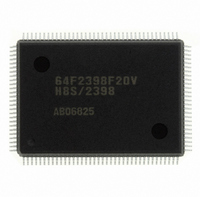
DF2398F20V Renesas Electronics America, DF2398F20V Datasheet - Page 546

DF2398F20V
Manufacturer Part Number
DF2398F20V
Description
IC H8S/2300 MCU FLASH 128QFP
Manufacturer
Renesas Electronics America
Series
H8® H8S/2300r
Specifications of DF2398F20V
Core Processor
H8S/2000
Core Size
16-Bit
Speed
20MHz
Connectivity
SCI, SmartCard
Peripherals
DMA, POR, PWM, WDT
Number Of I /o
87
Program Memory Size
256KB (256K x 8)
Program Memory Type
FLASH
Ram Size
8K x 8
Voltage - Supply (vcc/vdd)
4.5 V ~ 5.5 V
Data Converters
A/D 8x10b; D/A 2x8b
Oscillator Type
Internal
Operating Temperature
-20°C ~ 75°C
Package / Case
128-QFP
For Use With
YR0K42378FC000BA - KIT EVAL FOR H8S/2378
Lead Free Status / RoHS Status
Lead free / RoHS Compliant
Eeprom Size
-
Available stocks
Company
Part Number
Manufacturer
Quantity
Price
Company:
Part Number:
DF2398F20V
Manufacturer:
Renesas Electronics America
Quantity:
135
Company:
Part Number:
DF2398F20V
Manufacturer:
Renesas Electronics America
Quantity:
10 000
- Current page: 546 of 1049
- Download datasheet (5Mb)
Where M : Reception margin (%)
Assuming values of F = 0 and D = 0.5 in formula (1), a reception margin of 46.875% is given by formula (2) below.
When D = 0.5 and F = 0,
M = (0.5 –
However, this is only the computed value, and a margin of 20% to 30% should be allowed in system design.
Restrictions on Use of DMAC or DTC
Operation before mode transition (for the H8S/2398, H8S/2394, H8S/2392, and H8S/2390)
Before a mode transition to module stop mode or software standby mode, SCR should be initialized first, then SMR, BRR,
and SCMR should be initialized.
Rev.6.00 Oct.28.2004 page 516 of 1016
REJ09B0138-0600H
= 46.875%
When an external clock source is used as the serial clock, the transmit clock should not be input until at least 5 ø clock
cycles after TDR is updated by the DMAC or DTC. Misoperation may occur if the transmit clock is input within 4 ø
clocks after TDR is updated. (Figure 14-22)
When RDR is read by the DMAC or DTC, be sure to set the activation source to the relevant SCI reception data full
interrupt (RXI).
N : Ratio of bit rate to clock (N = 16)
D : Clock duty (D = 0 to 1.0)
L : Frame length (L = 9 to 12)
F : Absolute value of clock rate deviation
2
SCK
TDRE
Serial data
Note: When operating on an external clock, set t >4 clocks.
1
16
Figure 14-22 Example of Clocked Synchronous Transmission by DTC
100%
t
LSB
D0
D1
D2
D3
D4
D5
... Formula (2)
D6
D7
Related parts for DF2398F20V
Image
Part Number
Description
Manufacturer
Datasheet
Request
R

Part Number:
Description:
CONN PLUG 12POS DUAL 0.5MM SMD
Manufacturer:
Hirose Electric Co Ltd
Datasheet:

Part Number:
Description:
CONN PLUG 18POS DUAL 0.5MM SMD
Manufacturer:
Hirose Electric Co Ltd
Datasheet:

Part Number:
Description:
CONN PLUG 14POS DUAL 0.5MM SMD
Manufacturer:
Hirose Electric Co Ltd
Datasheet:

Part Number:
Description:
CONN RECEPT 20POS DUAL 0.5MM SMD
Manufacturer:
Hirose Electric Co Ltd
Datasheet:

Part Number:
Description:
CONN PLUG 16POS DUAL 0.5MM SMD
Manufacturer:
Hirose Electric Co Ltd
Datasheet:

Part Number:
Description:
CONN RECEPT 16POS DUAL 0.5MM SMD
Manufacturer:
Hirose Electric Co Ltd
Datasheet:

Part Number:
Description:
CONN PLUG 20POS DUAL 0.5MM SMD
Manufacturer:
Hirose Electric Co Ltd
Datasheet:

Part Number:
Description:
CONN PLUG 30POS DUAL 0.5MM SMD
Manufacturer:
Hirose Electric Co Ltd
Datasheet:

Part Number:
Description:
CONN RECEPT 30POS DUAL 0.5MM SMD
Manufacturer:
Hirose Electric Co Ltd
Datasheet:

Part Number:
Description:
CONN PLUG 40POS DUAL 0.5MM SMD
Manufacturer:
Hirose Electric Co Ltd
Datasheet:

Part Number:
Description:
KIT STARTER FOR M16C/29
Manufacturer:
Renesas Electronics America
Datasheet:

Part Number:
Description:
KIT STARTER FOR R8C/2D
Manufacturer:
Renesas Electronics America
Datasheet:

Part Number:
Description:
R0K33062P STARTER KIT
Manufacturer:
Renesas Electronics America
Datasheet:

Part Number:
Description:
KIT STARTER FOR R8C/23 E8A
Manufacturer:
Renesas Electronics America
Datasheet:

Part Number:
Description:
KIT STARTER FOR R8C/25
Manufacturer:
Renesas Electronics America
Datasheet:


