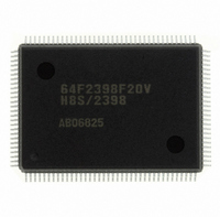
DF2398F20V Renesas Electronics America, DF2398F20V Datasheet - Page 683

DF2398F20V
Manufacturer Part Number
DF2398F20V
Description
IC H8S/2300 MCU FLASH 128QFP
Manufacturer
Renesas Electronics America
Series
H8® H8S/2300r
Specifications of DF2398F20V
Core Processor
H8S/2000
Core Size
16-Bit
Speed
20MHz
Connectivity
SCI, SmartCard
Peripherals
DMA, POR, PWM, WDT
Number Of I /o
87
Program Memory Size
256KB (256K x 8)
Program Memory Type
FLASH
Ram Size
8K x 8
Voltage - Supply (vcc/vdd)
4.5 V ~ 5.5 V
Data Converters
A/D 8x10b; D/A 2x8b
Oscillator Type
Internal
Operating Temperature
-20°C ~ 75°C
Package / Case
128-QFP
For Use With
YR0K42378FC000BA - KIT EVAL FOR H8S/2378
Lead Free Status / RoHS Status
Lead free / RoHS Compliant
Eeprom Size
-
Available stocks
Company
Part Number
Manufacturer
Quantity
Price
Company:
Part Number:
DF2398F20V
Manufacturer:
Renesas Electronics America
Quantity:
135
Company:
Part Number:
DF2398F20V
Manufacturer:
Renesas Electronics America
Quantity:
10 000
- Current page: 683 of 1049
- Download datasheet (5Mb)
19.22.5 Auto-Program Mode
In auto-program mode, 128 bytes are programmed simultaneously. For this purpose, 128 consecutive byte data
transfers should be performed.
A 128-byte data transfer must be performed even if writing fewer than 128 bytes; in this case, H'FF data must be
written to the extra addresses.
The lower 7 bits of the transfer address must be held low. If an invalid address is input, memory programming will be
started but a programming error will occur.
Memory address transfer is executed in the second cycle (figure 19-59). Do not perform transfer later than the second
cycle.
Do not perform a command write during a programming operation.
Perform one auto-programming operation for a 128-byte block for each address. One or more additional programming
operations cannot be carried out on address blocks that have already been programmed.
Confirm normal end of auto-programming by checking I/O
purpose (the I/O
Status polling I/O
has not been performed, reading is possible by enabling CE and OE.
I/O
I/O
A
A
7
7
18
18
to I/O
to I/O
to A
to A
7
WE
WE
CE
OE
OE
CE
status polling pin is used to identify the end of an auto-program operation).
6
0
0
and I/O
0
0
VIH
VIH
VIL
VIL
Figure 19-57 Timing Waveforms for CE/OE Enable State Read
Figure 19-58 Timing Waveforms for CE/OE Clocked Read
7
information is retained until the next command write. As long as the next command write
Address stable
t
acc
t
Address stable
acc
t
ce
t
oe
t
oh
t
oh
6
. Alternatively, status read mode can also be used for this
t
df
t
Address stable
acc
Address stable
t
acc
t
ce
Rev.6.00 Oct.28.2004 page 653 of 1016
t
oe
t
oh
t
oh
t
df
REJ09B0138-0600H
Related parts for DF2398F20V
Image
Part Number
Description
Manufacturer
Datasheet
Request
R

Part Number:
Description:
CONN PLUG 12POS DUAL 0.5MM SMD
Manufacturer:
Hirose Electric Co Ltd
Datasheet:

Part Number:
Description:
CONN PLUG 18POS DUAL 0.5MM SMD
Manufacturer:
Hirose Electric Co Ltd
Datasheet:

Part Number:
Description:
CONN PLUG 14POS DUAL 0.5MM SMD
Manufacturer:
Hirose Electric Co Ltd
Datasheet:

Part Number:
Description:
CONN RECEPT 20POS DUAL 0.5MM SMD
Manufacturer:
Hirose Electric Co Ltd
Datasheet:

Part Number:
Description:
CONN PLUG 16POS DUAL 0.5MM SMD
Manufacturer:
Hirose Electric Co Ltd
Datasheet:

Part Number:
Description:
CONN RECEPT 16POS DUAL 0.5MM SMD
Manufacturer:
Hirose Electric Co Ltd
Datasheet:

Part Number:
Description:
CONN PLUG 20POS DUAL 0.5MM SMD
Manufacturer:
Hirose Electric Co Ltd
Datasheet:

Part Number:
Description:
CONN PLUG 30POS DUAL 0.5MM SMD
Manufacturer:
Hirose Electric Co Ltd
Datasheet:

Part Number:
Description:
CONN RECEPT 30POS DUAL 0.5MM SMD
Manufacturer:
Hirose Electric Co Ltd
Datasheet:

Part Number:
Description:
CONN PLUG 40POS DUAL 0.5MM SMD
Manufacturer:
Hirose Electric Co Ltd
Datasheet:

Part Number:
Description:
KIT STARTER FOR M16C/29
Manufacturer:
Renesas Electronics America
Datasheet:

Part Number:
Description:
KIT STARTER FOR R8C/2D
Manufacturer:
Renesas Electronics America
Datasheet:

Part Number:
Description:
R0K33062P STARTER KIT
Manufacturer:
Renesas Electronics America
Datasheet:

Part Number:
Description:
KIT STARTER FOR R8C/23 E8A
Manufacturer:
Renesas Electronics America
Datasheet:

Part Number:
Description:
KIT STARTER FOR R8C/25
Manufacturer:
Renesas Electronics America
Datasheet:


