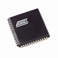
AT89C5131A-S3SUL Atmel, AT89C5131A-S3SUL Datasheet - Page 116

AT89C5131A-S3SUL
Manufacturer Part Number
AT89C5131A-S3SUL
Description
MCU 8051 32K FLASH USB 52-PLCC
Manufacturer
Atmel
Series
AT89C513xr
Specifications of AT89C5131A-S3SUL
Core Processor
C52X2
Core Size
8-Bit
Speed
48MHz
Connectivity
I²C, SPI, UART/USART, USB
Peripherals
LED, POR, PWM, WDT
Number Of I /o
34
Program Memory Size
32KB (32K x 8)
Program Memory Type
FLASH
Eeprom Size
4K x 8
Ram Size
1.25K x 8
Voltage - Supply (vcc/vdd)
3 V ~ 3.6 V
Oscillator Type
Internal
Operating Temperature
-40°C ~ 85°C
Package / Case
52-PLCC
Processor Series
AT89x
Core
8051
Data Bus Width
8 bit
Data Ram Size
1.25 KB
Interface Type
2-Wire, EUART, SPI, USB
Maximum Clock Frequency
48 MHz
Number Of Programmable I/os
34
Number Of Timers
3 bit
Operating Supply Voltage
3 V to 3.6 V
Maximum Operating Temperature
+ 85 C
Mounting Style
SMD/SMT
3rd Party Development Tools
PK51, CA51, A51, ULINK2
Development Tools By Supplier
AT89STK-05
Minimum Operating Temperature
- 40 C
For Use With
AT89STK-10 - KIT EVAL APPL MASS STORAGEAT89STK-05 - KIT STARTER FOR AT89C5131
Lead Free Status / RoHS Status
Lead free / RoHS Compliant
Data Converters
-
Lead Free Status / Rohs Status
Details
Available stocks
Company
Part Number
Manufacturer
Quantity
Price
- Current page: 116 of 186
- Download datasheet (2Mb)
USB Controller
Description
Figure 56. USB Device Controller Block Diagram
116
AT89C5131A-L
D+
D-
USB
D+/D-
Buffer
DPLL
.
The USB device controller provides the hardware that the AT89C5131 needs to inter-
face a USB link to a data flow stored in a double port memory (DPRAM).
The USB controller requires a 48 MHz ±0.25% reference clock, which is the output of
the AT89C5131 PLL (see Section “PLL”, page 14) divided by a clock prescaler. This
clock is used to generate a 12 MHz Full-speed bit clock from the received USB differen-
tial data and to transmit data according to full speed USB device tolerance. Clock
recovery is done by a Digital Phase Locked Loop (DPLL) block, which is compliant with
the jitter specification of the USB bus.
The Serial Interface Engine (SIE) block performs NRZI encoding and decoding, bit stuff-
ing, CRC generation and checking, and the serial-parallel data conversion.
The Universal Function Interface (UFI) realizes the interface between the data flow and
the Dual Port RAM.
SIE
48 MHz
12 MHz
+/- 0.25%
UFI
C51
Microcontroller
Interface
Up to 48 MHz
UC_sysclk
4338F–USB–08/07
Related parts for AT89C5131A-S3SUL
Image
Part Number
Description
Manufacturer
Datasheet
Request
R

Part Number:
Description:
Manufacturer:
Atmel Corporation
Datasheet:

Part Number:
Description:
Manufacturer:
Atmel Corporation
Datasheet:

Part Number:
Description:
IC 8051 MCU FLASH 32K USB 32QFN
Manufacturer:
Atmel
Datasheet:

Part Number:
Description:
IC 8051 MCU FLASH 32K USB 52PLCC
Manufacturer:
Atmel
Datasheet:

Part Number:
Description:
IC MCU 32KB 3-3.6V USB 48-VQFN
Manufacturer:
Atmel
Datasheet:

Part Number:
Description:
MCU 8051 32K FLASH USB 28-SOIC
Manufacturer:
Atmel
Datasheet:

Part Number:
Description:
IC 8051 MCU FLASH 32K USB 64VQFP
Manufacturer:
Atmel
Datasheet:

Part Number:
Description:
MCU 8051 32K FLASH USB 64-VQFP
Manufacturer:
Atmel
Datasheet:

Part Number:
Description:
MCU 8051 32K FLASH USB 28-SOIC
Manufacturer:
Atmel
Datasheet:

Part Number:
Description:
IC 8051 MCU FLASH 32K USB 48QFN
Manufacturer:
Atmel
Datasheet:

Part Number:
Description:
IC 8051 MCU FLASH 32K USB 64VQFP
Manufacturer:
Atmel
Datasheet:

Part Number:
Description:
IC 8051 MCU FLASH 32K USB 32QFN
Manufacturer:
Atmel
Datasheet:

Part Number:
Description:
IC 8051 MCU FLASH 32K USB 52PLCC
Manufacturer:
Atmel
Datasheet:

Part Number:
Description:
IC 8051 MCU FLASH 32K USB 28SOIC
Manufacturer:
Atmel
Datasheet:


