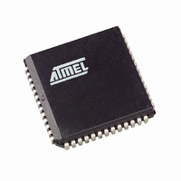
AT89C5131A-S3SUL Atmel, AT89C5131A-S3SUL Datasheet - Page 7

AT89C5131A-S3SUL
Manufacturer Part Number
AT89C5131A-S3SUL
Description
MCU 8051 32K FLASH USB 52-PLCC
Manufacturer
Atmel
Series
AT89C513xr
Specifications of AT89C5131A-S3SUL
Core Processor
C52X2
Core Size
8-Bit
Speed
48MHz
Connectivity
I²C, SPI, UART/USART, USB
Peripherals
LED, POR, PWM, WDT
Number Of I /o
34
Program Memory Size
32KB (32K x 8)
Program Memory Type
FLASH
Eeprom Size
4K x 8
Ram Size
1.25K x 8
Voltage - Supply (vcc/vdd)
3 V ~ 3.6 V
Oscillator Type
Internal
Operating Temperature
-40°C ~ 85°C
Package / Case
52-PLCC
Processor Series
AT89x
Core
8051
Data Bus Width
8 bit
Data Ram Size
1.25 KB
Interface Type
2-Wire, EUART, SPI, USB
Maximum Clock Frequency
48 MHz
Number Of Programmable I/os
34
Number Of Timers
3 bit
Operating Supply Voltage
3 V to 3.6 V
Maximum Operating Temperature
+ 85 C
Mounting Style
SMD/SMT
3rd Party Development Tools
PK51, CA51, A51, ULINK2
Development Tools By Supplier
AT89STK-05
Minimum Operating Temperature
- 40 C
For Use With
AT89STK-10 - KIT EVAL APPL MASS STORAGEAT89STK-05 - KIT STARTER FOR AT89C5131
Lead Free Status / RoHS Status
Lead free / RoHS Compliant
Data Converters
-
Lead Free Status / Rohs Status
Details
Available stocks
Company
Part Number
Manufacturer
Quantity
Price
- Current page: 7 of 186
- Download datasheet (2Mb)
4338F–USB–08/07
Table 4. Timer 0, Timer 1 and Timer 2 Signal Description (Continued)
Table 5. LED Signal Description
Table 6. TWI Signal Description
Table 7. SPI Signal Description
LED[3:0]
Signal
Signal
Name
Name
Signal
Signal
Name
Name
T2EX
MISO
MOSI
SCK
SCL
SDA
SS
T0
T1
T2
Type
Type
Type
Type
I/O
I/O
I/O
I/O
O
I/O
I/O
I
I
I
I
O
Description
Timer Counter 0 External Clock Input
When Timer 0 operates as a counter, a falling edge on the T0 pin
increments the count.
Timer/Counter 1 External Clock Input
When Timer 1 operates as a counter, a falling edge on the T1 pin
increments the count.
Timer/Counter 2 External Clock Input
Timer/Counter 2 Clock Output
Timer/Counter 2 Reload/Capture/Direction Control Input
Description
SS: SPI Slave Select
MISO: SPI Master Input Slave Output line
When SPI is in master mode, MISO receives data from the slave
peripheral. When SPI is in slave mode, MISO outputs data to the master
controller.
SCK: SPI Serial Clock
SCK outputs clock to the slave peripheral or receive clock from the master
MOSI: SPI Master Output Slave Input line
When SPI is in master mode, MOSI outputs data to the slave peripheral.
When SPI is in slave mode, MOSI receives data from the master controller
Description
Direct Drive LED Output
These pins can be directly connected to the Cathode of standard LEDs
without external current limiting resistors. The typical current of each
output can be programmed by software to 2, 6 or 10 mA. Several outputs
can be connected together to get higher drive capabilities.
Description
SCL: TWI Serial Clock
SCL output the serial clock to slave peripherals.
SCL input the serial clock from master.
SDA: TWI Serial Data
SCL is the bidirectional TWI data line.
Alternate
Alternate
Alternate
Alternate
Function
Function
Function
Function
P3.4
P3.5
P1.0
P1.1
P3.3
P3.5
P3.6
P3.7
P4.0
P4.1
P1.1
P1.5
P1.6
P1.7
7
Related parts for AT89C5131A-S3SUL
Image
Part Number
Description
Manufacturer
Datasheet
Request
R

Part Number:
Description:
Manufacturer:
Atmel Corporation
Datasheet:

Part Number:
Description:
Manufacturer:
Atmel Corporation
Datasheet:

Part Number:
Description:
IC 8051 MCU FLASH 32K USB 32QFN
Manufacturer:
Atmel
Datasheet:

Part Number:
Description:
IC 8051 MCU FLASH 32K USB 52PLCC
Manufacturer:
Atmel
Datasheet:

Part Number:
Description:
IC MCU 32KB 3-3.6V USB 48-VQFN
Manufacturer:
Atmel
Datasheet:

Part Number:
Description:
MCU 8051 32K FLASH USB 28-SOIC
Manufacturer:
Atmel
Datasheet:

Part Number:
Description:
IC 8051 MCU FLASH 32K USB 64VQFP
Manufacturer:
Atmel
Datasheet:

Part Number:
Description:
MCU 8051 32K FLASH USB 64-VQFP
Manufacturer:
Atmel
Datasheet:

Part Number:
Description:
MCU 8051 32K FLASH USB 28-SOIC
Manufacturer:
Atmel
Datasheet:

Part Number:
Description:
IC 8051 MCU FLASH 32K USB 48QFN
Manufacturer:
Atmel
Datasheet:

Part Number:
Description:
IC 8051 MCU FLASH 32K USB 64VQFP
Manufacturer:
Atmel
Datasheet:

Part Number:
Description:
IC 8051 MCU FLASH 32K USB 32QFN
Manufacturer:
Atmel
Datasheet:

Part Number:
Description:
IC 8051 MCU FLASH 32K USB 52PLCC
Manufacturer:
Atmel
Datasheet:

Part Number:
Description:
IC 8051 MCU FLASH 32K USB 28SOIC
Manufacturer:
Atmel
Datasheet:


