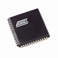
AT89C5131A-S3SUL Atmel, AT89C5131A-S3SUL Datasheet - Page 126

AT89C5131A-S3SUL
Manufacturer Part Number
AT89C5131A-S3SUL
Description
MCU 8051 32K FLASH USB 52-PLCC
Manufacturer
Atmel
Series
AT89C513xr
Specifications of AT89C5131A-S3SUL
Core Processor
C52X2
Core Size
8-Bit
Speed
48MHz
Connectivity
I²C, SPI, UART/USART, USB
Peripherals
LED, POR, PWM, WDT
Number Of I /o
34
Program Memory Size
32KB (32K x 8)
Program Memory Type
FLASH
Eeprom Size
4K x 8
Ram Size
1.25K x 8
Voltage - Supply (vcc/vdd)
3 V ~ 3.6 V
Oscillator Type
Internal
Operating Temperature
-40°C ~ 85°C
Package / Case
52-PLCC
Processor Series
AT89x
Core
8051
Data Bus Width
8 bit
Data Ram Size
1.25 KB
Interface Type
2-Wire, EUART, SPI, USB
Maximum Clock Frequency
48 MHz
Number Of Programmable I/os
34
Number Of Timers
3 bit
Operating Supply Voltage
3 V to 3.6 V
Maximum Operating Temperature
+ 85 C
Mounting Style
SMD/SMT
3rd Party Development Tools
PK51, CA51, A51, ULINK2
Development Tools By Supplier
AT89STK-05
Minimum Operating Temperature
- 40 C
For Use With
AT89STK-10 - KIT EVAL APPL MASS STORAGEAT89STK-05 - KIT STARTER FOR AT89C5131
Lead Free Status / RoHS Status
Lead free / RoHS Compliant
Data Converters
-
Lead Free Status / Rohs Status
Details
Available stocks
Company
Part Number
Manufacturer
Quantity
Price
Control Transactions
Setup Stage
Data Stage: Control Endpoint
Direction
Status Stage
126
AT89C5131A-L
The DIR bit in the UEPSTAX register will be at 0.
Receiving Setup packets is the same as receiving Bulk Out packets, except that the
RXSETUP bit in the UEPSTAX register is set by the USB controller instead of the
RXOUTB0 bit to indicate that an Out packet with a Setup PID has been received on the
Control endpoint. When the RXSETUP bit has been set, all the other bits of the UEP-
STAX register are cleared and an interrupt is triggered if enabled.
The firmware has to read the Setup request stored in the Control endpoint FIFO before
clearing the RXSETUP bit to free the endpoint FIFO for the next transaction.
The data stage management is similar to Bulk management.
A Control endpoint is managed by the USB controller as a full-duplex endpoint: IN and
OUT. All other endpoint types are managed as half-duplex endpoint: IN or OUT. The
firmware has to specify the control endpoint direction for the data stage using the DIR bit
in the UEPSTAX register.
The firmware has to use the DIR bit before data IN in order to meet the data-toggle
requirements:
•
•
To send a STALL handshake, see “STALL Handshake” on page 129.
The DIR bit in the UEPSTAX register will be reset at 0 for IN and OUT status stage.
The status stage management is similar to Bulk management.
•
•
If the data stage consists of INs,
the firmware has to set the DIR bit in the UEPSTAX register before writing into the
FIFO and sending the data by setting to 1 the TXRDY bit in the UEPSTAX register.
The IN transaction is complete when the TXCMPL has been set by the hardware.
The firmware will clear the TXCMPL bit before any other transaction.
If the data stage consists of OUTs,
the firmware has to leave the DIR bit at 0. The RXOUTB0 bit is set by hardware
when a new valid packet has been received on the endpoint. The firmware must
read the data stored into the FIFO and then clear the RXOUTB0 bit to reset the
FIFO and to allow the next transaction.
For a Control Write transaction or a No-Data Control transaction, the status stage
consists of a IN Zero Length Packet (see “Bulk/Interrupt IN Transactions in
Standard Mode” on page 124). To send a STALL handshake, see “STALL
Handshake” on page 129.
For a Control Read transaction, the status stage consists of a OUT Zero Length
Packet (see “Bulk/Interrupt OUT Transactions in Standard Mode” on page 122).
4338F–USB–08/07


