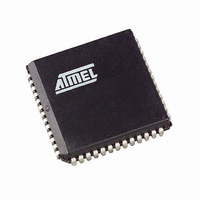
AT89C5131A-S3SUL Atmel, AT89C5131A-S3SUL Datasheet - Page 43

AT89C5131A-S3SUL
Manufacturer Part Number
AT89C5131A-S3SUL
Description
MCU 8051 32K FLASH USB 52-PLCC
Manufacturer
Atmel
Series
AT89C513xr
Specifications of AT89C5131A-S3SUL
Core Processor
C52X2
Core Size
8-Bit
Speed
48MHz
Connectivity
I²C, SPI, UART/USART, USB
Peripherals
LED, POR, PWM, WDT
Number Of I /o
34
Program Memory Size
32KB (32K x 8)
Program Memory Type
FLASH
Eeprom Size
4K x 8
Ram Size
1.25K x 8
Voltage - Supply (vcc/vdd)
3 V ~ 3.6 V
Oscillator Type
Internal
Operating Temperature
-40°C ~ 85°C
Package / Case
52-PLCC
Processor Series
AT89x
Core
8051
Data Bus Width
8 bit
Data Ram Size
1.25 KB
Interface Type
2-Wire, EUART, SPI, USB
Maximum Clock Frequency
48 MHz
Number Of Programmable I/os
34
Number Of Timers
3 bit
Operating Supply Voltage
3 V to 3.6 V
Maximum Operating Temperature
+ 85 C
Mounting Style
SMD/SMT
3rd Party Development Tools
PK51, CA51, A51, ULINK2
Development Tools By Supplier
AT89STK-05
Minimum Operating Temperature
- 40 C
For Use With
AT89STK-10 - KIT EVAL APPL MASS STORAGEAT89STK-05 - KIT STARTER FOR AT89C5131
Lead Free Status / RoHS Status
Lead free / RoHS Compliant
Data Converters
-
Lead Free Status / Rohs Status
Details
Available stocks
Company
Part Number
Manufacturer
Quantity
Price
- Current page: 43 of 186
- Download datasheet (2Mb)
In-System
Programming (ISP)
Flash Programming and
Erasure
4338F–USB–08/07
With the implementation of the User Space (FM0) and the Boot Space (FM1) in Flash
technology the AT89C5131 allows the system engineer the development of applications
with a very high level of flexibility. This flexibility is based on the possibility to alter the
customer program at any stages of a product’s life:
•
•
Note:
This ISP allows code modification over the total lifetime of the product.
Besides the default Bootloaders Atmel provide customers all the needed Application-
Programming-Interfaces (API) which are needed for the ISP. The API are located in the
Boot memory.
This allow the customer to have a full use of the 32-Kbyte user memory.
There are three methods for programming the Flash memory:
•
•
•
Figure 22. Flash Memory Mapping
Before mounting the chip on the PCB, FM0 flash can be programmed with the
application code. FM1 is always preprogrammed by Atmel with a USB bootloader.
Once the chip is mounted on the PCB, it can be programmed by serial mode via the
USB bus.
The Atmel bootloader located in FM1 is activated by the application. Low level API
routines (located in FM1)will be used to program FM0. The interface used for serial
downloading to FM0 is the USB. API can be called also by user’s bootloader located
in FM0 at [SBV]00h.
A further method exist in activating the Atmel boot loader by hardware activation.
See the Section “Hardware Registers”.
The FM0 can be programmed also by the parallel mode using a programmer.
[SBV]00h
1. The user can also program his own bootloader in FM1.
7FFFh
0000h
Flash Memory
32K Bytes
Custom
Bootloader
FM0
F400h
FM1 Mapped between F400h and FFFFh
when API Called
3K Bytes IAP
Bootloader
FM1
FFFFh
43
(1)
Related parts for AT89C5131A-S3SUL
Image
Part Number
Description
Manufacturer
Datasheet
Request
R

Part Number:
Description:
Manufacturer:
Atmel Corporation
Datasheet:

Part Number:
Description:
Manufacturer:
Atmel Corporation
Datasheet:

Part Number:
Description:
IC 8051 MCU FLASH 32K USB 32QFN
Manufacturer:
Atmel
Datasheet:

Part Number:
Description:
IC 8051 MCU FLASH 32K USB 52PLCC
Manufacturer:
Atmel
Datasheet:

Part Number:
Description:
IC MCU 32KB 3-3.6V USB 48-VQFN
Manufacturer:
Atmel
Datasheet:

Part Number:
Description:
MCU 8051 32K FLASH USB 28-SOIC
Manufacturer:
Atmel
Datasheet:

Part Number:
Description:
IC 8051 MCU FLASH 32K USB 64VQFP
Manufacturer:
Atmel
Datasheet:

Part Number:
Description:
MCU 8051 32K FLASH USB 64-VQFP
Manufacturer:
Atmel
Datasheet:

Part Number:
Description:
MCU 8051 32K FLASH USB 28-SOIC
Manufacturer:
Atmel
Datasheet:

Part Number:
Description:
IC 8051 MCU FLASH 32K USB 48QFN
Manufacturer:
Atmel
Datasheet:

Part Number:
Description:
IC 8051 MCU FLASH 32K USB 64VQFP
Manufacturer:
Atmel
Datasheet:

Part Number:
Description:
IC 8051 MCU FLASH 32K USB 32QFN
Manufacturer:
Atmel
Datasheet:

Part Number:
Description:
IC 8051 MCU FLASH 32K USB 52PLCC
Manufacturer:
Atmel
Datasheet:

Part Number:
Description:
IC 8051 MCU FLASH 32K USB 28SOIC
Manufacturer:
Atmel
Datasheet:


