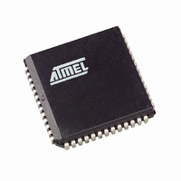
AT89C5131A-S3SUL Atmel, AT89C5131A-S3SUL Datasheet - Page 38

AT89C5131A-S3SUL
Manufacturer Part Number
AT89C5131A-S3SUL
Description
MCU 8051 32K FLASH USB 52-PLCC
Manufacturer
Atmel
Series
AT89C513xr
Specifications of AT89C5131A-S3SUL
Core Processor
C52X2
Core Size
8-Bit
Speed
48MHz
Connectivity
I²C, SPI, UART/USART, USB
Peripherals
LED, POR, PWM, WDT
Number Of I /o
34
Program Memory Size
32KB (32K x 8)
Program Memory Type
FLASH
Eeprom Size
4K x 8
Ram Size
1.25K x 8
Voltage - Supply (vcc/vdd)
3 V ~ 3.6 V
Oscillator Type
Internal
Operating Temperature
-40°C ~ 85°C
Package / Case
52-PLCC
Processor Series
AT89x
Core
8051
Data Bus Width
8 bit
Data Ram Size
1.25 KB
Interface Type
2-Wire, EUART, SPI, USB
Maximum Clock Frequency
48 MHz
Number Of Programmable I/os
34
Number Of Timers
3 bit
Operating Supply Voltage
3 V to 3.6 V
Maximum Operating Temperature
+ 85 C
Mounting Style
SMD/SMT
3rd Party Development Tools
PK51, CA51, A51, ULINK2
Development Tools By Supplier
AT89STK-05
Minimum Operating Temperature
- 40 C
For Use With
AT89STK-10 - KIT EVAL APPL MASS STORAGEAT89STK-05 - KIT STARTER FOR AT89C5131
Lead Free Status / RoHS Status
Lead free / RoHS Compliant
Data Converters
-
Lead Free Status / Rohs Status
Details
Available stocks
Company
Part Number
Manufacturer
Quantity
Price
Default Values
Software Registers
38
AT89C5131A-L
Table 38. Program Lock bits
Notes:
These security bits protect the code access through the parallel programming interface.
They are set by default to level 4. The code access through the ISP is still possible and
is controlled by the “software security bits” which are stored in the extra Flash memory
accessed by the ISP firmware.
To load a new application with the parallel programmer, a chip erase must be done first.
This will set the HSB in its inactive state and will erase the Flash memory. The part ref-
erence can always be read using Flash parallel programming modes.
The default value of the HSB provides parts ready to be programmed with ISP:
•
•
•
•
Several registers are used, in factory and by parallel programmers, to make copies of
hardware registers contents. These values are used by Atmel ISP (see Section “In-Sys-
tem Programming (ISP)”).
These registers are in the “Extra Flash Memory” part of the Flash memory. This block is
also called ”XAF” or eXtra Array Flash. They are accessed in the following ways:
•
•
•
Several software registers are described in Table 39.
Security level
BLJB: Cleared to force ISP operation.
X2: Set to force X1 mode (Standard Mode)
OSCON1-0: Set to start with 32 MHz oscillator configuration value.
LB2-0: Security level four to protect the code from a parallel access with maximum
security.
Commands issued by the parallel memory programmer.
Commands issued by the ISP software.
Calls of API issued by the application software.
1
2
3
4
1. U: unprogrammed or “one” level.
2. P: programmed or “zero” level.
3. X: don’t care
4. WARNING: Security level 2 and 3 should only be programmed after verification.
Program Lock Bits
LB0
U
P
X
X
LB1
U
U
P
X
LB2
U
U
U
P
Protection Description
No program lock features enabled.
MOVC instruction executed from external
program memory is disabled from fetching code
bytes from any internal memory, EA is sampled
and latched on reset, and further parallel
programming of the Flash and of the EEPROM
(boot and Xdata) is disabled. ISP and software
programming with API are still allowed.
Same as 2, also verify through parallel
programming interface is disabled and serial
programming ISP is still allowed.
Same as 3, also external execution is disabled.
4338F–USB–08/07


