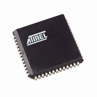
AT89C5131A-S3SUL Atmel, AT89C5131A-S3SUL Datasheet - Page 41

AT89C5131A-S3SUL
Manufacturer Part Number
AT89C5131A-S3SUL
Description
MCU 8051 32K FLASH USB 52-PLCC
Manufacturer
Atmel
Series
AT89C513xr
Specifications of AT89C5131A-S3SUL
Core Processor
C52X2
Core Size
8-Bit
Speed
48MHz
Connectivity
I²C, SPI, UART/USART, USB
Peripherals
LED, POR, PWM, WDT
Number Of I /o
34
Program Memory Size
32KB (32K x 8)
Program Memory Type
FLASH
Eeprom Size
4K x 8
Ram Size
1.25K x 8
Voltage - Supply (vcc/vdd)
3 V ~ 3.6 V
Oscillator Type
Internal
Operating Temperature
-40°C ~ 85°C
Package / Case
52-PLCC
Processor Series
AT89x
Core
8051
Data Bus Width
8 bit
Data Ram Size
1.25 KB
Interface Type
2-Wire, EUART, SPI, USB
Maximum Clock Frequency
48 MHz
Number Of Programmable I/os
34
Number Of Timers
3 bit
Operating Supply Voltage
3 V to 3.6 V
Maximum Operating Temperature
+ 85 C
Mounting Style
SMD/SMT
3rd Party Development Tools
PK51, CA51, A51, ULINK2
Development Tools By Supplier
AT89STK-05
Minimum Operating Temperature
- 40 C
For Use With
AT89STK-10 - KIT EVAL APPL MASS STORAGEAT89STK-05 - KIT STARTER FOR AT89C5131
Lead Free Status / RoHS Status
Lead free / RoHS Compliant
Data Converters
-
Lead Free Status / Rohs Status
Details
Available stocks
Company
Part Number
Manufacturer
Quantity
Price
EEPROM Data Memory
Description
Write Data in the Column
Latches
Programming
Read Data
4338F–USB–08/07
The 1-Kbyte on-chip EEPROM memory block is located at addresses 0000h to 03FFh of
the ERAM memory space and is selected by setting control bits in the EECON register.
A read in the EEPROM memory is done with a MOVX instruction.
A physical write in the EEPROM memory is done in two steps: write data in the column
latches and transfer of all data latches into an EEPROM memory row (programming).
The number of data written on the page may vary from 1 to 128 bytes (the page size).
When programming, only the data written in the column latch is programmed and a ninth
bit is used to obtain this feature. This provides the capability to program the whole mem-
ory by bytes, by page or by a number of bytes in a page. Indeed, each ninth bit is set
when the writing the corresponding byte in a row and all these ninth bits are reset after
the writing of the complete EEPROM row.
Data is written by byte to the column latches as for an external RAM memory. Out of the
11 address bits of the data pointer, the 4 MSBs are used for page selection (row) and 7
are used for byte selection. Between two EEPROM programming sessions, all the
addresses in the column latches must stay on the same page, meaning that the 4 MSB
must not be changed.
The following procedure is used to write to the column latches:
•
•
•
•
•
The EEPROM programming consists on the following actions:
•
•
•
•
The following procedure is used to read the data stored in the EEPROM memory:
•
•
•
•
Set bit EEE of EECON register
Load DPTR with the address to write
Store A register with the data to be written
Execute a MOVX @DPTR, A
If needed, loop the three last instructions until the end of a 128 bytes page
Writing one or more bytes of one page in the column latches. Normally, all bytes
must belong to the same page; if not, the first page address will be latched and the
others discarded.
Launching programming by writing the control sequence (52h followed by A2h) to
the EECON register.
EEBUSY flag in EECON is then set by hardware to indicate that programming is in
progress and that the EEPROM segment is not available for reading.
The end of programming is indicated by a hardware clear of the EEBUSY flag.
Set bit EEE of EECON register
Stretch the MOVX to accommodate the slow access time of the column latch (Set bit
M0 of AUXR register)
Load DPTR with the address to read
Execute a MOVX A, @DPTR
41


