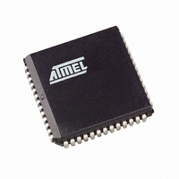
AT89C5131A-S3SUL Atmel, AT89C5131A-S3SUL Datasheet - Page 40

AT89C5131A-S3SUL
Manufacturer Part Number
AT89C5131A-S3SUL
Description
MCU 8051 32K FLASH USB 52-PLCC
Manufacturer
Atmel
Series
AT89C513xr
Specifications of AT89C5131A-S3SUL
Core Processor
C52X2
Core Size
8-Bit
Speed
48MHz
Connectivity
I²C, SPI, UART/USART, USB
Peripherals
LED, POR, PWM, WDT
Number Of I /o
34
Program Memory Size
32KB (32K x 8)
Program Memory Type
FLASH
Eeprom Size
4K x 8
Ram Size
1.25K x 8
Voltage - Supply (vcc/vdd)
3 V ~ 3.6 V
Oscillator Type
Internal
Operating Temperature
-40°C ~ 85°C
Package / Case
52-PLCC
Processor Series
AT89x
Core
8051
Data Bus Width
8 bit
Data Ram Size
1.25 KB
Interface Type
2-Wire, EUART, SPI, USB
Maximum Clock Frequency
48 MHz
Number Of Programmable I/os
34
Number Of Timers
3 bit
Operating Supply Voltage
3 V to 3.6 V
Maximum Operating Temperature
+ 85 C
Mounting Style
SMD/SMT
3rd Party Development Tools
PK51, CA51, A51, ULINK2
Development Tools By Supplier
AT89STK-05
Minimum Operating Temperature
- 40 C
For Use With
AT89STK-10 - KIT EVAL APPL MASS STORAGEAT89STK-05 - KIT STARTER FOR AT89C5131
Lead Free Status / RoHS Status
Lead free / RoHS Compliant
Data Converters
-
Lead Free Status / Rohs Status
Details
Available stocks
Company
Part Number
Manufacturer
Quantity
Price
- Current page: 40 of 186
- Download datasheet (2Mb)
Flash Memory Status
Figure 21. Flash Memory Possible Contents
Memory Organization
40
0000h
AT89C5131A-L
7FFFh AT89C5131A-M
Default
Virgin
After ISP
Application
Table 41. Program Lock Bits of the SSB
Notes:
AT89C5131A-L parts are delivered with the ISP boot in the Flash memory. After ISP or
parallel programming, the possible contents of the Flash memory are summarized in
Figure 21:
In the AT89C5131A-L, the lowest 32K of the 64 Kbyte program memory address space
is filled by internal Flash.
When the EA is pin high, the processor fetches instructions from internal program Flash.
Bus expansion for accessing program memory from 32K upward is automatic since
external instruction fetches occur automatically when the program counter exceeds
7FFFh (32K). If the EA pin is tied low, all program memory fetches are from external
memory. If all storage is on chip, then byte location 7FFFh (32K) should be left vacant to
prevent and undesired pre-fetch from external program memory address 8000h (32K).
Security
Level
Program Lock Bits
1
2
3
1. U: unprogrammed or "one" level.
2. P: programmed or “zero” level.
3. WARNING: Security level 2 and 3 should only be programmed after Flash and code
verification.
LB0
U
P
P
Dedicated
ISP
After ISP
Application
Virgin
LB1
U
U
P
or
Protection Description
No program lock features enabled.
ISP programming of the Flash is disabled.
Same as 2, also verify through ISP programming interface is disabled.
After parallel
programming
Application
After parallel
programming
Dedicated
ISP
Application
Virgin
or
After parallel
programming
Application
Virgin
or
4338F–USB–08/07
Related parts for AT89C5131A-S3SUL
Image
Part Number
Description
Manufacturer
Datasheet
Request
R

Part Number:
Description:
Manufacturer:
Atmel Corporation
Datasheet:

Part Number:
Description:
Manufacturer:
Atmel Corporation
Datasheet:

Part Number:
Description:
IC 8051 MCU FLASH 32K USB 32QFN
Manufacturer:
Atmel
Datasheet:

Part Number:
Description:
IC 8051 MCU FLASH 32K USB 52PLCC
Manufacturer:
Atmel
Datasheet:

Part Number:
Description:
IC MCU 32KB 3-3.6V USB 48-VQFN
Manufacturer:
Atmel
Datasheet:

Part Number:
Description:
MCU 8051 32K FLASH USB 28-SOIC
Manufacturer:
Atmel
Datasheet:

Part Number:
Description:
IC 8051 MCU FLASH 32K USB 64VQFP
Manufacturer:
Atmel
Datasheet:

Part Number:
Description:
MCU 8051 32K FLASH USB 64-VQFP
Manufacturer:
Atmel
Datasheet:

Part Number:
Description:
MCU 8051 32K FLASH USB 28-SOIC
Manufacturer:
Atmel
Datasheet:

Part Number:
Description:
IC 8051 MCU FLASH 32K USB 48QFN
Manufacturer:
Atmel
Datasheet:

Part Number:
Description:
IC 8051 MCU FLASH 32K USB 64VQFP
Manufacturer:
Atmel
Datasheet:

Part Number:
Description:
IC 8051 MCU FLASH 32K USB 32QFN
Manufacturer:
Atmel
Datasheet:

Part Number:
Description:
IC 8051 MCU FLASH 32K USB 52PLCC
Manufacturer:
Atmel
Datasheet:

Part Number:
Description:
IC 8051 MCU FLASH 32K USB 28SOIC
Manufacturer:
Atmel
Datasheet:


