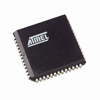
AT89C5131A-S3SUL Atmel, AT89C5131A-S3SUL Datasheet - Page 121

AT89C5131A-S3SUL
Manufacturer Part Number
AT89C5131A-S3SUL
Description
MCU 8051 32K FLASH USB 52-PLCC
Manufacturer
Atmel
Series
AT89C513xr
Specifications of AT89C5131A-S3SUL
Core Processor
C52X2
Core Size
8-Bit
Speed
48MHz
Connectivity
I²C, SPI, UART/USART, USB
Peripherals
LED, POR, PWM, WDT
Number Of I /o
34
Program Memory Size
32KB (32K x 8)
Program Memory Type
FLASH
Eeprom Size
4K x 8
Ram Size
1.25K x 8
Voltage - Supply (vcc/vdd)
3 V ~ 3.6 V
Oscillator Type
Internal
Operating Temperature
-40°C ~ 85°C
Package / Case
52-PLCC
Processor Series
AT89x
Core
8051
Data Bus Width
8 bit
Data Ram Size
1.25 KB
Interface Type
2-Wire, EUART, SPI, USB
Maximum Clock Frequency
48 MHz
Number Of Programmable I/os
34
Number Of Timers
3 bit
Operating Supply Voltage
3 V to 3.6 V
Maximum Operating Temperature
+ 85 C
Mounting Style
SMD/SMT
3rd Party Development Tools
PK51, CA51, A51, ULINK2
Development Tools By Supplier
AT89STK-05
Minimum Operating Temperature
- 40 C
For Use With
AT89STK-10 - KIT EVAL APPL MASS STORAGEAT89STK-05 - KIT STARTER FOR AT89C5131
Lead Free Status / RoHS Status
Lead free / RoHS Compliant
Data Converters
-
Lead Free Status / Rohs Status
Details
Available stocks
Company
Part Number
Manufacturer
Quantity
Price
Read/Write Data FIFO
FIFO Mapping
Figure 61. Endpoint FIFO Configuration
Read Data FIFO
Write Data FIFO
4338F–USB–08/07
Endpoint 0
Endpoint 6
UEPSTA0
UEPSTA6
•
Depending on the selected endpoint through the UEPNUM register, the UEPDATX reg-
ister allows to access the corresponding endpoint data fifo.
The read access for each OUT endpoint is performed using the UEPDATX register.
After a new valid packet has been received on an Endpoint, the data are stored into the
FIFO and the byte counter of the endpoint is updated (UBYCTLX and UBYCTHX regis-
ters). The firmware has to store the endpoint byte counter before any access to the
endpoint FIFO. The byte counter is not updated when reading the FIFO.
To read data from an endpoint, select the correct endpoint number in UEPNUM and
read the UEPDATX register. This action automatically decreases the corresponding
address vector, and the next data is then available in the UEPDATX register.
The write access for each IN endpoint is performed using the UEPDATX register.
To write a byte into an IN endpoint FIFO, select the correct endpoint number in UEP-
NUM and write into the UEPDATX register. The corresponding address vector is
automatically increased, and another write can be carried out.
Warning 1: The byte counter is not updated.
Warning 2: Do not write more bytes than supported by the corresponding endpoint.
UBYCTH0
UBYCTH6
Endpoint FIFO reset
Before using an endpoint, its FIFO will be reset. This action resets the FIFO pointer
to its original value, resets the byte counter of the endpoint (UBYCTLX and
UBYCTHX registers), and resets the data toggle bit (DTGL bit in UEPCONX).
The reset of an endpoint FIFO is performed by setting to 1 and resetting to 0 the
corresponding bit in the UEPRST register.
For example, in order to reset the Endpoint number 2 FIFO, write 0000 0100b then
0000 0000b in the UEPRST register.
Note that the endpoint reset doesn’t reset the bank number for ping-pong endpoints.
UEPCON0
UEPCON6
UBYCTL0
UBYCTL6
UEPDAT0
UEPDAT6
UEPNUM
0
1
2
3
4
5
6
X
UEPSTAX
UBYCTHX
SFR registers
UEPCONX
UBYCTLX
UEPDATX
121


