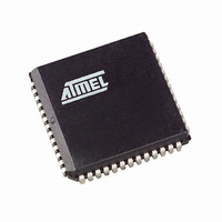
AT89C5131A-S3SUL Atmel, AT89C5131A-S3SUL Datasheet - Page 13

AT89C5131A-S3SUL
Manufacturer Part Number
AT89C5131A-S3SUL
Description
MCU 8051 32K FLASH USB 52-PLCC
Manufacturer
Atmel
Series
AT89C513xr
Specifications of AT89C5131A-S3SUL
Core Processor
C52X2
Core Size
8-Bit
Speed
48MHz
Connectivity
I²C, SPI, UART/USART, USB
Peripherals
LED, POR, PWM, WDT
Number Of I /o
34
Program Memory Size
32KB (32K x 8)
Program Memory Type
FLASH
Eeprom Size
4K x 8
Ram Size
1.25K x 8
Voltage - Supply (vcc/vdd)
3 V ~ 3.6 V
Oscillator Type
Internal
Operating Temperature
-40°C ~ 85°C
Package / Case
52-PLCC
Processor Series
AT89x
Core
8051
Data Bus Width
8 bit
Data Ram Size
1.25 KB
Interface Type
2-Wire, EUART, SPI, USB
Maximum Clock Frequency
48 MHz
Number Of Programmable I/os
34
Number Of Timers
3 bit
Operating Supply Voltage
3 V to 3.6 V
Maximum Operating Temperature
+ 85 C
Mounting Style
SMD/SMT
3rd Party Development Tools
PK51, CA51, A51, ULINK2
Development Tools By Supplier
AT89STK-05
Minimum Operating Temperature
- 40 C
For Use With
AT89STK-10 - KIT EVAL APPL MASS STORAGEAT89STK-05 - KIT STARTER FOR AT89C5131
Lead Free Status / RoHS Status
Lead free / RoHS Compliant
Data Converters
-
Lead Free Status / Rohs Status
Details
Available stocks
Company
Part Number
Manufacturer
Quantity
Price
- Current page: 13 of 186
- Download datasheet (2Mb)
Clock Controller
Introduction
Figure 7. Oscillator Block Diagram
Oscillator
4338F–USB–08/07
X1
X2
PLLCON.2
EXT48
PCON.1
PD
The AT89C5131A-L clock controller is based on an on-chip oscillator feeding an on-chip
Phase Lock Loop (PLL). All the internal clocks to the peripherals and CPU core are gen-
erated by this controller.
The AT89C5131A-L X1 and X2 pins are the input and the output of a single-stage on-
chip inverter (see Figure 7) that can be configured with off-chip components as a Pierce
oscillator (see Figure 8). Value of capacitors and crystal characteristics are detailed in
the section “DC Characteristics”.
The X1 pin can also be used as input for an external 48 MHz clock.
The clock controller outputs three different clocks as shown in Figure 7:
•
•
•
These clocks are enabled or disabled depending on the power reduction mode as
detailed in Section “Power Management”, page 152.
Two clock sources are available for CPU:
•
•
In order to optimize the power consumption, the oscillator inverter is inactive when the
PLL output is not selected for the USB device.
a clock for the CPU core
a clock for the peripherals which is used to generate the Timers, PCA, WD, and Port
sampling clocks
a clock for the USB controller
Crystal oscillator on X1 and X2 pins: Up to 32 MHz
External 48 MHz clock on X1 pin
PLL
0
1
÷
2
CKCON.0
X2
0
1
PCON.0
IDL
USB
Clock
Peripheral
Clock
CPU Core
Clock
13
Related parts for AT89C5131A-S3SUL
Image
Part Number
Description
Manufacturer
Datasheet
Request
R

Part Number:
Description:
Manufacturer:
Atmel Corporation
Datasheet:

Part Number:
Description:
Manufacturer:
Atmel Corporation
Datasheet:

Part Number:
Description:
IC 8051 MCU FLASH 32K USB 32QFN
Manufacturer:
Atmel
Datasheet:

Part Number:
Description:
IC 8051 MCU FLASH 32K USB 52PLCC
Manufacturer:
Atmel
Datasheet:

Part Number:
Description:
IC MCU 32KB 3-3.6V USB 48-VQFN
Manufacturer:
Atmel
Datasheet:

Part Number:
Description:
MCU 8051 32K FLASH USB 28-SOIC
Manufacturer:
Atmel
Datasheet:

Part Number:
Description:
IC 8051 MCU FLASH 32K USB 64VQFP
Manufacturer:
Atmel
Datasheet:

Part Number:
Description:
MCU 8051 32K FLASH USB 64-VQFP
Manufacturer:
Atmel
Datasheet:

Part Number:
Description:
MCU 8051 32K FLASH USB 28-SOIC
Manufacturer:
Atmel
Datasheet:

Part Number:
Description:
IC 8051 MCU FLASH 32K USB 48QFN
Manufacturer:
Atmel
Datasheet:

Part Number:
Description:
IC 8051 MCU FLASH 32K USB 64VQFP
Manufacturer:
Atmel
Datasheet:

Part Number:
Description:
IC 8051 MCU FLASH 32K USB 32QFN
Manufacturer:
Atmel
Datasheet:

Part Number:
Description:
IC 8051 MCU FLASH 32K USB 52PLCC
Manufacturer:
Atmel
Datasheet:

Part Number:
Description:
IC 8051 MCU FLASH 32K USB 28SOIC
Manufacturer:
Atmel
Datasheet:


