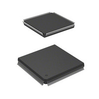
HD6417750SF200V Renesas Electronics America, HD6417750SF200V Datasheet - Page 188

HD6417750SF200V
Manufacturer Part Number
HD6417750SF200V
Description
MPU 3V 16K PB-FREE 208-QFP
Manufacturer
Renesas Electronics America
Series
SuperH® SH7750r
Datasheet
1.D6417750RBP240DV.pdf
(1164 pages)
Specifications of HD6417750SF200V
Core Processor
SH-4
Core Size
32-Bit
Speed
200MHz
Connectivity
EBI/EMI, FIFO, SCI, SmartCard
Peripherals
DMA, POR, WDT
Number Of I /o
28
Program Memory Type
ROMless
Ram Size
24K x 8
Voltage - Supply (vcc/vdd)
1.8 V ~ 2.07 V
Oscillator Type
External
Operating Temperature
-20°C ~ 75°C
Package / Case
208-QFP
Lead Free Status / RoHS Status
Lead free / RoHS Compliant
Eeprom Size
-
Program Memory Size
-
Data Converters
-
Available stocks
Company
Part Number
Manufacturer
Quantity
Price
Company:
Part Number:
HD6417750SF200V
Manufacturer:
Renesas Electronics America
Quantity:
10 000
- Current page: 188 of 1164
- Download datasheet (7Mb)
Section 3 Memory Management Unit (MMU)
Software Processing (Initial Page Write Exception Handling Routine): The following
processing should be carried out as the responsibility of software:
1. Retrieve the necessary page table entry from external memory.
2. Write 1 to the D bit in the external memory page table entry.
3. Write to PTEL the values of the PPN, PR, SZ, C, D, WT, SH, and V bits in the page table
4. When the entry to be replaced in entry replacement is specified by software, write that value to
5. Execute the LDTLB instruction and write the contents of PTEH, PTEL, and PTEA to the
6. Finally, execute the exception handling return instruction (RTE), terminate the exception
3.7
To enable the ITLB and UTLB to be managed by software, their contents can be read and written
by a P2 area program with a MOV instruction in privileged mode. Operation is not guaranteed if
access is made from a program in another area. A branch to an area other than the P2 area should
be made at least 8 instructions after this MOV instruction. The ITLB and UTLB are allocated to
the P4 area in physical memory space. VPN, V, and ASID in the ITLB can be accessed as an
address array, PPN, V, SZ, PR, C, and SH as data array 1, and SA and TC as data array 2. VPN,
D, V, and ASID in the UTLB can be accessed as an address array, PPN, V, SZ, PR, C, D, WT, and
SH as data array 1, and SA and TC as data array 2. V and D can be accessed from both the address
array side and the data array side. Only longword access is possible. Instruction fetches cannot be
performed in these areas. For reserved bits, a write value of 0 should be specified; their read value
is undefined.
Rev.7.00 Oct. 10, 2008 Page 102 of 1074
REJ09B0366-0700
entry recorded in external memory. If necessary, the values of the SA and TC bits should be
written to PTEA.
URC in the MMUCR register. If URC is greater than URB at this time, the value should be
changed to an appropriate value after issuing an LDTLB instruction.
UTLB.
handling routine, and return control to the normal flow. The RTE instruction should be issued
at least one instruction after the LDTLB instruction.
Memory-Mapped TLB Configuration
Related parts for HD6417750SF200V
Image
Part Number
Description
Manufacturer
Datasheet
Request
R

Part Number:
Description:
KIT STARTER FOR M16C/29
Manufacturer:
Renesas Electronics America
Datasheet:

Part Number:
Description:
KIT STARTER FOR R8C/2D
Manufacturer:
Renesas Electronics America
Datasheet:

Part Number:
Description:
R0K33062P STARTER KIT
Manufacturer:
Renesas Electronics America
Datasheet:

Part Number:
Description:
KIT STARTER FOR R8C/23 E8A
Manufacturer:
Renesas Electronics America
Datasheet:

Part Number:
Description:
KIT STARTER FOR R8C/25
Manufacturer:
Renesas Electronics America
Datasheet:

Part Number:
Description:
KIT STARTER H8S2456 SHARPE DSPLY
Manufacturer:
Renesas Electronics America
Datasheet:

Part Number:
Description:
KIT STARTER FOR R8C38C
Manufacturer:
Renesas Electronics America
Datasheet:

Part Number:
Description:
KIT STARTER FOR R8C35C
Manufacturer:
Renesas Electronics America
Datasheet:

Part Number:
Description:
KIT STARTER FOR R8CL3AC+LCD APPS
Manufacturer:
Renesas Electronics America
Datasheet:

Part Number:
Description:
KIT STARTER FOR RX610
Manufacturer:
Renesas Electronics America
Datasheet:

Part Number:
Description:
KIT STARTER FOR R32C/118
Manufacturer:
Renesas Electronics America
Datasheet:

Part Number:
Description:
KIT DEV RSK-R8C/26-29
Manufacturer:
Renesas Electronics America
Datasheet:

Part Number:
Description:
KIT STARTER FOR SH7124
Manufacturer:
Renesas Electronics America
Datasheet:

Part Number:
Description:
KIT STARTER FOR H8SX/1622
Manufacturer:
Renesas Electronics America
Datasheet:

Part Number:
Description:
KIT DEV FOR SH7203
Manufacturer:
Renesas Electronics America
Datasheet:


