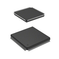
HD6417750SF200V Renesas Electronics America, HD6417750SF200V Datasheet - Page 629

HD6417750SF200V
Manufacturer Part Number
HD6417750SF200V
Description
MPU 3V 16K PB-FREE 208-QFP
Manufacturer
Renesas Electronics America
Series
SuperH® SH7750r
Datasheet
1.D6417750RBP240DV.pdf
(1164 pages)
Specifications of HD6417750SF200V
Core Processor
SH-4
Core Size
32-Bit
Speed
200MHz
Connectivity
EBI/EMI, FIFO, SCI, SmartCard
Peripherals
DMA, POR, WDT
Number Of I /o
28
Program Memory Type
ROMless
Ram Size
24K x 8
Voltage - Supply (vcc/vdd)
1.8 V ~ 2.07 V
Oscillator Type
External
Operating Temperature
-20°C ~ 75°C
Package / Case
208-QFP
Lead Free Status / RoHS Status
Lead free / RoHS Compliant
Eeprom Size
-
Program Memory Size
-
Data Converters
-
Available stocks
Company
Part Number
Manufacturer
Quantity
Price
Company:
Part Number:
HD6417750SF200V
Manufacturer:
Renesas Electronics America
Quantity:
10 000
- Current page: 629 of 1164
- Download datasheet (7Mb)
13.3.16 Notes on Usage
Refresh: Auto refresh operations stop when a transition is made to standby mode, hardware
standby mode or deep-sleep mode. If the memory system requires refresh operations, set the
memory in the self-refresh state prior to making the transition to standby mode, hardware standby
mode or deep-sleep mode.
Bus Arbitration: On transition to standby mode or deep-sleep mode, the processor in master
mode does not release bus privileges. In systems performing bus arbitration, make the transition to
standby mode or deep-sleep mode only after setting the bus privilege release enable bit
(BCR1.BREQEN) to 0 for the processor in master mode. If the bus privilege release enable bit
remains set to 1, operation cannot be guaranteed when the transition is made to standby mode or
deep-sleep mode.
Synchronous DRAM Mode Register Setting (SH7750, SH7750S Only): The following
conditions must be satisfied when setting the synchronous DRAM mode register.
• The DMAC must not be activated until synchronous DRAM mode register setting is
• Register setting for the on-chip peripheral modules*
Notes: 1. If a conflict occurs between synchronous DRAM mode register setting and memory
BSREQ Output in Partial-Sharing Master Mode: When conditions a. to d. below are all
satisfied, the BSREQ pin may be driven low during a refresh operation and a bus release request
issued to the master mode device, even though there was no request to access area 2. The period
that BSREQ is asserted is 3 to 21 CKIO cycles, as specified by the setting of MCR.TRC (see d.
below).
completed.*
DRAM mode register setting is completed.*
2. This applies to the following on-chip peripheral modules: CPG, RTC, INTC, TMU,
3. If synchronous DRAM mode register setting is performed immediately following write
access using the DMAC, neither operation can be guaranteed.
SCI, SCIF, and H-UDI.
access to the on-chip peripheral modules*
modules cannot be guaranteed. Note that following power-on, synchronous DRAM
mode register settings should be performed before accessing synchronous DRAM.
After making mode register settings, do not change them.
1
3
2
, the values written to the on-chip peripheral
2
Rev.7.00 Oct. 10, 2008 Page 543 of 1074
must not be performed until synchronous
Section 13 Bus State Controller (BSC)
REJ09B0366-0700
Related parts for HD6417750SF200V
Image
Part Number
Description
Manufacturer
Datasheet
Request
R

Part Number:
Description:
KIT STARTER FOR M16C/29
Manufacturer:
Renesas Electronics America
Datasheet:

Part Number:
Description:
KIT STARTER FOR R8C/2D
Manufacturer:
Renesas Electronics America
Datasheet:

Part Number:
Description:
R0K33062P STARTER KIT
Manufacturer:
Renesas Electronics America
Datasheet:

Part Number:
Description:
KIT STARTER FOR R8C/23 E8A
Manufacturer:
Renesas Electronics America
Datasheet:

Part Number:
Description:
KIT STARTER FOR R8C/25
Manufacturer:
Renesas Electronics America
Datasheet:

Part Number:
Description:
KIT STARTER H8S2456 SHARPE DSPLY
Manufacturer:
Renesas Electronics America
Datasheet:

Part Number:
Description:
KIT STARTER FOR R8C38C
Manufacturer:
Renesas Electronics America
Datasheet:

Part Number:
Description:
KIT STARTER FOR R8C35C
Manufacturer:
Renesas Electronics America
Datasheet:

Part Number:
Description:
KIT STARTER FOR R8CL3AC+LCD APPS
Manufacturer:
Renesas Electronics America
Datasheet:

Part Number:
Description:
KIT STARTER FOR RX610
Manufacturer:
Renesas Electronics America
Datasheet:

Part Number:
Description:
KIT STARTER FOR R32C/118
Manufacturer:
Renesas Electronics America
Datasheet:

Part Number:
Description:
KIT DEV RSK-R8C/26-29
Manufacturer:
Renesas Electronics America
Datasheet:

Part Number:
Description:
KIT STARTER FOR SH7124
Manufacturer:
Renesas Electronics America
Datasheet:

Part Number:
Description:
KIT STARTER FOR H8SX/1622
Manufacturer:
Renesas Electronics America
Datasheet:

Part Number:
Description:
KIT DEV FOR SH7203
Manufacturer:
Renesas Electronics America
Datasheet:


