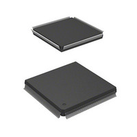
HD6417750SF200V Renesas Electronics America, HD6417750SF200V Datasheet - Page 443

HD6417750SF200V
Manufacturer Part Number
HD6417750SF200V
Description
MPU 3V 16K PB-FREE 208-QFP
Manufacturer
Renesas Electronics America
Series
SuperH® SH7750r
Datasheet
1.D6417750RBP240DV.pdf
(1164 pages)
Specifications of HD6417750SF200V
Core Processor
SH-4
Core Size
32-Bit
Speed
200MHz
Connectivity
EBI/EMI, FIFO, SCI, SmartCard
Peripherals
DMA, POR, WDT
Number Of I /o
28
Program Memory Type
ROMless
Ram Size
24K x 8
Voltage - Supply (vcc/vdd)
1.8 V ~ 2.07 V
Oscillator Type
External
Operating Temperature
-20°C ~ 75°C
Package / Case
208-QFP
Lead Free Status / RoHS Status
Lead free / RoHS Compliant
Eeprom Size
-
Program Memory Size
-
Data Converters
-
Available stocks
Company
Part Number
Manufacturer
Quantity
Price
Company:
Part Number:
HD6417750SF200V
Manufacturer:
Renesas Electronics America
Quantity:
10 000
- Current page: 443 of 1164
- Download datasheet (7Mb)
13.1
The functions of the bus state controller (BSC) include division of the external memory space, and
output of control signals in accordance with various types of memory and bus interface
specifications. The BSC functions allow DRAM, synchronous DRAM, SRAM, ROM, etc., to be
connected to this LSI, and also support the PCMCIA interface protocol, enabling system design to
be simplified and data transfers to be carried out at high speed by a compact system.
13.1.1
The BSC has the following features:
• External memory space is managed as 7 independent areas
• SRAM interface
• DRAM interface
⎯ Maximum 64 Mbytes for each of areas 0 to 6
⎯ Bus width of each area can be set in a register (except area 0, which uses an external pin
⎯ Wait state insertion by RDY pin
⎯ Wait state insertion can be controlled by program
⎯ Specification of types of memory connectable to each area
⎯ Output the control signals of memory to each area
⎯ Automatic wait cycle insertion to prevent data bus collisions in case of consecutive
⎯ Write strobe setup time and hold time periods can be inserted in a write cycle to enable
⎯ Wait state insertion can be controlled by program
⎯ Wait state insertion by RDY pin
⎯ Row address/column address multiplexing according to DRAM capacity
⎯ Burst operation (fast page mode, EDO mode)
⎯ CAS-before-RAS refresh and self-refresh
setting)
memory accesses to different areas, or a read access followed by a write access to the same
area
connection to low-speed memory
Connectable areas: 0 to 6
Settable bus widths: 64, 32, 16, 8
Overview
Features
Section 13 Bus State Controller (BSC)
Rev.7.00 Oct. 10, 2008 Page 357 of 1074
Section 13 Bus State Controller (BSC)
REJ09B0366-0700
Related parts for HD6417750SF200V
Image
Part Number
Description
Manufacturer
Datasheet
Request
R

Part Number:
Description:
KIT STARTER FOR M16C/29
Manufacturer:
Renesas Electronics America
Datasheet:

Part Number:
Description:
KIT STARTER FOR R8C/2D
Manufacturer:
Renesas Electronics America
Datasheet:

Part Number:
Description:
R0K33062P STARTER KIT
Manufacturer:
Renesas Electronics America
Datasheet:

Part Number:
Description:
KIT STARTER FOR R8C/23 E8A
Manufacturer:
Renesas Electronics America
Datasheet:

Part Number:
Description:
KIT STARTER FOR R8C/25
Manufacturer:
Renesas Electronics America
Datasheet:

Part Number:
Description:
KIT STARTER H8S2456 SHARPE DSPLY
Manufacturer:
Renesas Electronics America
Datasheet:

Part Number:
Description:
KIT STARTER FOR R8C38C
Manufacturer:
Renesas Electronics America
Datasheet:

Part Number:
Description:
KIT STARTER FOR R8C35C
Manufacturer:
Renesas Electronics America
Datasheet:

Part Number:
Description:
KIT STARTER FOR R8CL3AC+LCD APPS
Manufacturer:
Renesas Electronics America
Datasheet:

Part Number:
Description:
KIT STARTER FOR RX610
Manufacturer:
Renesas Electronics America
Datasheet:

Part Number:
Description:
KIT STARTER FOR R32C/118
Manufacturer:
Renesas Electronics America
Datasheet:

Part Number:
Description:
KIT DEV RSK-R8C/26-29
Manufacturer:
Renesas Electronics America
Datasheet:

Part Number:
Description:
KIT STARTER FOR SH7124
Manufacturer:
Renesas Electronics America
Datasheet:

Part Number:
Description:
KIT STARTER FOR H8SX/1622
Manufacturer:
Renesas Electronics America
Datasheet:

Part Number:
Description:
KIT DEV FOR SH7203
Manufacturer:
Renesas Electronics America
Datasheet:


