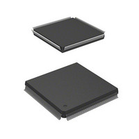
HD6417750SF200V Renesas Electronics America, HD6417750SF200V Datasheet - Page 672

HD6417750SF200V
Manufacturer Part Number
HD6417750SF200V
Description
MPU 3V 16K PB-FREE 208-QFP
Manufacturer
Renesas Electronics America
Series
SuperH® SH7750r
Datasheet
1.D6417750RBP240DV.pdf
(1164 pages)
Specifications of HD6417750SF200V
Core Processor
SH-4
Core Size
32-Bit
Speed
200MHz
Connectivity
EBI/EMI, FIFO, SCI, SmartCard
Peripherals
DMA, POR, WDT
Number Of I /o
28
Program Memory Type
ROMless
Ram Size
24K x 8
Voltage - Supply (vcc/vdd)
1.8 V ~ 2.07 V
Oscillator Type
External
Operating Temperature
-20°C ~ 75°C
Package / Case
208-QFP
Lead Free Status / RoHS Status
Lead free / RoHS Compliant
Eeprom Size
-
Program Memory Size
-
Data Converters
-
Available stocks
Company
Part Number
Manufacturer
Quantity
Price
Company:
Part Number:
HD6417750SF200V
Manufacturer:
Renesas Electronics America
Quantity:
10 000
- Current page: 672 of 1164
- Download datasheet (7Mb)
Section 14 Direct Memory Access Controller (DMAC)
Operation: Figures 14.12 to 14.22 show the timing in each mode.
1. Cycle Steal Mode
2. Burst Mode, Dual Address Mode, Level Detection
3. Burst Mode, Single Address Mode, Level Detection
Rev.7.00 Oct. 10, 2008 Page 586 of 1074
REJ09B0366-0700
In cycle steal mode, The DREQ sampling timing differs for dual address mode and single
address mode, and for level detection and edge detection of DREQ.
For example, in figure 14.12 (cycle steal mode, dual address mode, level detection), DMAC
transfer begins, at the earliest, four CKIO cycles after the first sampling operation. The second
sampling operation is performed one cycle after the start of the first DMAC transfer write
cycle. If DREQ is not detected at this time, sampling is executed in every subsequent cycle.
In figure 14.13 (cycle steal mode, dual address mode, edge detection), DMAC transfer begins,
at the earliest, five CKIO cycles after the first sampling operation. The second sampling
operation begins from the cycle in which the first DMAC transfer read cycle ends. If DREQ is
not detected at this time, sampling is executed in every subsequent cycle.
For details of the timing for various kinds of memory access, see section 13, Bus State
Controller (BSC).
Figure 14.18 shows the case of cycle steal mode, single address mode, and level detection. In
this case, too, transfer is started, at the earliest, four CKIO cycles after the first DREQ
sampling operation. The second sampling operation is performed one cycle after the start of
the first DMAC transfer bus cycle.
Figure 14.19 shows the case of cycle steal mode, single address mode, and edge detection. In
this case, transfer is started, at the earliest, five CKIO cycles after the first DREQ sampling
operation. The second sampling begins one cycle after the first assertion of DRAK.
In single address mode, the DACK signal is output every DMAC transfer cycle.
DREQ sampling timing in burst mode using dual address mode and level detection is virtually
the same as for cycle steal mode.
For example, in figure 14.14, DMAC transfer begins, at the earliest, four CKIO cycles after the
first sampling operation. The second sampling operation is performed one cycle after the start
of the first DMAC transfer write cycle.
In the case of dual address mode transfer initiated by an external request, the DACK signal can
be output in either the read cycle or the write cycle of the DMAC transfer according to the
specification of the AM bit in CHCR.
DREQ sampling timing in burst mode using single address mode and level detection is shown
in figure 14.20.
Related parts for HD6417750SF200V
Image
Part Number
Description
Manufacturer
Datasheet
Request
R

Part Number:
Description:
KIT STARTER FOR M16C/29
Manufacturer:
Renesas Electronics America
Datasheet:

Part Number:
Description:
KIT STARTER FOR R8C/2D
Manufacturer:
Renesas Electronics America
Datasheet:

Part Number:
Description:
R0K33062P STARTER KIT
Manufacturer:
Renesas Electronics America
Datasheet:

Part Number:
Description:
KIT STARTER FOR R8C/23 E8A
Manufacturer:
Renesas Electronics America
Datasheet:

Part Number:
Description:
KIT STARTER FOR R8C/25
Manufacturer:
Renesas Electronics America
Datasheet:

Part Number:
Description:
KIT STARTER H8S2456 SHARPE DSPLY
Manufacturer:
Renesas Electronics America
Datasheet:

Part Number:
Description:
KIT STARTER FOR R8C38C
Manufacturer:
Renesas Electronics America
Datasheet:

Part Number:
Description:
KIT STARTER FOR R8C35C
Manufacturer:
Renesas Electronics America
Datasheet:

Part Number:
Description:
KIT STARTER FOR R8CL3AC+LCD APPS
Manufacturer:
Renesas Electronics America
Datasheet:

Part Number:
Description:
KIT STARTER FOR RX610
Manufacturer:
Renesas Electronics America
Datasheet:

Part Number:
Description:
KIT STARTER FOR R32C/118
Manufacturer:
Renesas Electronics America
Datasheet:

Part Number:
Description:
KIT DEV RSK-R8C/26-29
Manufacturer:
Renesas Electronics America
Datasheet:

Part Number:
Description:
KIT STARTER FOR SH7124
Manufacturer:
Renesas Electronics America
Datasheet:

Part Number:
Description:
KIT STARTER FOR H8SX/1622
Manufacturer:
Renesas Electronics America
Datasheet:

Part Number:
Description:
KIT DEV FOR SH7203
Manufacturer:
Renesas Electronics America
Datasheet:


