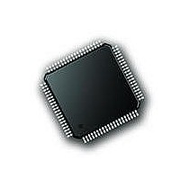
PIC18F87J72-I/PT Microchip Technology, PIC18F87J72-I/PT Datasheet - Page 283

PIC18F87J72-I/PT
Manufacturer Part Number
PIC18F87J72-I/PT
Description
IC PIC MCU 8BIT 14KB FLSH 80TQFP
Manufacturer
Microchip Technology
Series
PIC® 18Fr
Datasheet
1.PIC18F86J72-IPT.pdf
(480 pages)
Specifications of PIC18F87J72-I/PT
Program Memory Type
FLASH
Program Memory Size
128KB (64K x 16)
Package / Case
80-TQFP
Core Processor
PIC
Core Size
8-Bit
Speed
48MHz
Connectivity
I²C, LIN, SPI, UART/USART
Peripherals
Brown-out Detect/Reset, LCD, LVD, POR, PWM, WDT
Number Of I /o
51
Ram Size
3.8K x 8
Voltage - Supply (vcc/vdd)
2 V ~ 3.6 V
Data Converters
A/D 12x12b
Oscillator Type
Internal
Operating Temperature
-40°C ~ 85°C
Data Bus Width
8 bit
Data Ram Size
4 KB
Interface Type
SPI, USART, SPI, I2C
Maximum Clock Frequency
8 MHz
Number Of Programmable I/os
51
Number Of Timers
4
Operating Supply Voltage
2 V to 3.6 V
Maximum Operating Temperature
+ 85 C
Mounting Style
SMD/SMT
Minimum Operating Temperature
- 40 C
On-chip Adc
14
Controller Family/series
PIC18F
No. Of I/o's
51
Ram Memory Size
3923Byte
Cpu Speed
48MHz
No. Of Timers
4
Rohs Compliant
Yes
Lead Free Status / RoHS Status
Lead free / RoHS Compliant
Lead Free Status / RoHS Status
Lead free / RoHS Compliant, Lead free / RoHS Compliant
Available stocks
Company
Part Number
Manufacturer
Quantity
Price
Company:
Part Number:
PIC18F87J72-I/PT
Manufacturer:
Microchip
Quantity:
210
Company:
Part Number:
PIC18F87J72-I/PT
Manufacturer:
Microchip Technology
Quantity:
10 000
- Current page: 283 of 480
- Download datasheet (5Mb)
22.0
The dual-channel, 24-bit Analog Front End (AFE) is an
integrated, high-performance analog subsystem that
has been tailored for energy metering and power
measurement applications. The AFE contains two
synchronous sampling Delta-Sigma Analog-to-Digital
Converters ( ADC), two PGAs, a phase delay
compensation block, an internal voltage reference and
a dedicated, high-speed 20 MHz SPI compatible serial
interface. A functional block diagram of the AFE is
shown in Figure 22-1.
The A/D Converters contain a proprietary dithering
algorithm for reduced Idle tones and improved THD.
Each converter is preceded by a PGA, allowing for
weak signal amplification and true differential voltage
inputs to the converters. This allows the AFE to inter-
face with a large variety of voltage and current sensors
including shunts, current transformers, Rogowski coils
and Hall effect sensors.
FIGURE 22-1:
2010 Microchip Technology Inc.
REFIN+/OUT+
REFIN -
CH0+
CH1+
CH0-
CH1-
DUAL-CHANNEL, 24-BIT
ANALOG FRONT END (AFE)
Monitoring
Reference
+
SV
Voltage
-
POR
DUAL-CHANNEL ANALOG FRONT END FUNCTIONAL DIAGRAM
DD
V
REF
VREFEXT
DUAL-DS ADC
V
REF
+
+
-
-
PGA
PGA
-/
V
REF
+
SDN<1:0>, RESET<1:0>, GAIN<7:0>
Modulator
Modulator
ANALOG DIGITAL
SAV
SAV
D-S
D-S
DD
SS
Preliminary
SV
SV
SINC
SINC
DD
F
SS
3
3
POR
Shifter
Phase
PIC18F87J72 FAMILY
AFE data and control functions are accessed through a
dedicated register map. The map contains 24-bit wide
data words for each ADC (readable as 8-bit registers),
as well as five writable control registers to program
amplifier gain, oversampling, phase, resolution, dither-
ing, shutdown, Reset and communication features.
Communication is largely simplified with various
continuous read modes that can be accessed through
the serial interface and with a separate data ready pin
that can directly be connected to a microcontroller’s
IRQ input.
Because of the complexity of and comprehensive
options available on the AFE, a detailed explanation of
all of its functional elements is not provided in this
chapter. These are described in Appendix B:
“Dual-Channel, 24-Bit AFE Reference”. This chapter
explains the important points of configuring and using
the AFE in a PIC18F8XJ72 based application. Direct
links to relevant information in the AFE reference are
provided throughout the chapter for the reader’s
convenience.
DATA_CH1<23:0>
DATA_CH0<23:0>
DMCLK/DRCLK
PHASE <7:0>
AMCLK
DMCLK
Digital SPI
Generation
Interface
Clock
OSR<1:0>
PRE<1:0>
MCLK
DS39979A-page 283
CLKIA
DR
SDOA
ARESET
SDIA
SCKA
CSA
Related parts for PIC18F87J72-I/PT
Image
Part Number
Description
Manufacturer
Datasheet
Request
R

Part Number:
Description:
Manufacturer:
Microchip Technology Inc.
Datasheet:

Part Number:
Description:
Manufacturer:
Microchip Technology Inc.
Datasheet:

Part Number:
Description:
Manufacturer:
Microchip Technology Inc.
Datasheet:

Part Number:
Description:
Manufacturer:
Microchip Technology Inc.
Datasheet:

Part Number:
Description:
Manufacturer:
Microchip Technology Inc.
Datasheet:

Part Number:
Description:
Manufacturer:
Microchip Technology Inc.
Datasheet:

Part Number:
Description:
Manufacturer:
Microchip Technology Inc.
Datasheet:

Part Number:
Description:
Manufacturer:
Microchip Technology Inc.
Datasheet:


