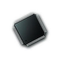
PIC18F87J72-I/PT Microchip Technology, PIC18F87J72-I/PT Datasheet - Page 457

PIC18F87J72-I/PT
Manufacturer Part Number
PIC18F87J72-I/PT
Description
IC PIC MCU 8BIT 14KB FLSH 80TQFP
Manufacturer
Microchip Technology
Series
PIC® 18Fr
Datasheet
1.PIC18F86J72-IPT.pdf
(480 pages)
Specifications of PIC18F87J72-I/PT
Program Memory Type
FLASH
Program Memory Size
128KB (64K x 16)
Package / Case
80-TQFP
Core Processor
PIC
Core Size
8-Bit
Speed
48MHz
Connectivity
I²C, LIN, SPI, UART/USART
Peripherals
Brown-out Detect/Reset, LCD, LVD, POR, PWM, WDT
Number Of I /o
51
Ram Size
3.8K x 8
Voltage - Supply (vcc/vdd)
2 V ~ 3.6 V
Data Converters
A/D 12x12b
Oscillator Type
Internal
Operating Temperature
-40°C ~ 85°C
Data Bus Width
8 bit
Data Ram Size
4 KB
Interface Type
SPI, USART, SPI, I2C
Maximum Clock Frequency
8 MHz
Number Of Programmable I/os
51
Number Of Timers
4
Operating Supply Voltage
2 V to 3.6 V
Maximum Operating Temperature
+ 85 C
Mounting Style
SMD/SMT
Minimum Operating Temperature
- 40 C
On-chip Adc
14
Controller Family/series
PIC18F
No. Of I/o's
51
Ram Memory Size
3923Byte
Cpu Speed
48MHz
No. Of Timers
4
Rohs Compliant
Yes
Lead Free Status / RoHS Status
Lead free / RoHS Compliant
Lead Free Status / RoHS Status
Lead free / RoHS Compliant, Lead free / RoHS Compliant
Available stocks
Company
Part Number
Manufacturer
Quantity
Price
Company:
Part Number:
PIC18F87J72-I/PT
Manufacturer:
Microchip
Quantity:
210
Company:
Part Number:
PIC18F87J72-I/PT
Manufacturer:
Microchip Technology
Quantity:
10 000
- Current page: 457 of 480
- Download datasheet (5Mb)
B.6.1
The ADC Channel Data Output registers always con-
tain the most recent A/D conversion data for each
channel. These registers are read-only. They can be
accessed independently as three 8-bit registers or
linked together (with READ<1:0> bits).
REGISTER B-1:
2010 Microchip Technology Inc.
bit 23
bit 15
bit 7
Legend:
R = Readable bit
-n = Value at POR
DATA_CHn
DATA_CHn
DATA_CHn
<23>
<15>
<7>
R-0
R-0
R-0
ADC CHANNEL DATA OUTPUT
REGISTERS
DATA_CHn
DATA_CHn
DATA_CHn
<22>
<14>
<6>
R-0
R-0
R-0
DATA_CHn: CHANNEL OUTPUT REGISTERS
(CH0, ADDRESSES 0x00-0x02; CH1; 0x03-0x05)
W = Writable bit
‘1’ = Bit is set
DATA_CHn
DATA_CHn
DATA_CHn
<21>
<13>
R-0
R-0
R-0
<5>
DATA_CHn
DATA_CHn
DATA_CHn
<20>
<12>
<4>
R-0
R-0
R-0
Preliminary
U = Unimplemented bit, read as ‘0’
‘0’ = Bit is cleared
DATA_CHn
DATA_CHn
DATA_CHn
PIC18F87J72 FAMILY
These registers are latched when an ADC read com-
munication occurs. When a data ready event occurs
during a read communication, the most current ADC
data is also latched to avoid data corruption issues.
The three bytes of each channel are updated synchro-
nously at a DRCLK rate. The three bytes can be
accessed separately if needed but are refreshed
synchronously.
<19>
<11>
<3>
R-0
R-0
R-0
DATA_CHn
DATA_CHn
DATA_CHn
<18>
<10>
<2>
R-0
R-0
R-0
x = Bit is unknown
DATA_CHn
DATA_CHn
DATA_CHn
<17>
<9>
<1>
R-0
R-0
R-0
DS39979A-page 457
DATA_CHn
DATA_CHn
DATA_CHn
<16>
<8>
<0>
R-0
R-0
R-0
bit 16
bit 8
bit 0
Related parts for PIC18F87J72-I/PT
Image
Part Number
Description
Manufacturer
Datasheet
Request
R

Part Number:
Description:
Manufacturer:
Microchip Technology Inc.
Datasheet:

Part Number:
Description:
Manufacturer:
Microchip Technology Inc.
Datasheet:

Part Number:
Description:
Manufacturer:
Microchip Technology Inc.
Datasheet:

Part Number:
Description:
Manufacturer:
Microchip Technology Inc.
Datasheet:

Part Number:
Description:
Manufacturer:
Microchip Technology Inc.
Datasheet:

Part Number:
Description:
Manufacturer:
Microchip Technology Inc.
Datasheet:

Part Number:
Description:
Manufacturer:
Microchip Technology Inc.
Datasheet:

Part Number:
Description:
Manufacturer:
Microchip Technology Inc.
Datasheet:


