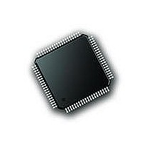
PIC18F87J72-I/PT Microchip Technology, PIC18F87J72-I/PT Datasheet - Page 447

PIC18F87J72-I/PT
Manufacturer Part Number
PIC18F87J72-I/PT
Description
IC PIC MCU 8BIT 14KB FLSH 80TQFP
Manufacturer
Microchip Technology
Series
PIC® 18Fr
Datasheet
1.PIC18F86J72-IPT.pdf
(480 pages)
Specifications of PIC18F87J72-I/PT
Program Memory Type
FLASH
Program Memory Size
128KB (64K x 16)
Package / Case
80-TQFP
Core Processor
PIC
Core Size
8-Bit
Speed
48MHz
Connectivity
I²C, LIN, SPI, UART/USART
Peripherals
Brown-out Detect/Reset, LCD, LVD, POR, PWM, WDT
Number Of I /o
51
Ram Size
3.8K x 8
Voltage - Supply (vcc/vdd)
2 V ~ 3.6 V
Data Converters
A/D 12x12b
Oscillator Type
Internal
Operating Temperature
-40°C ~ 85°C
Data Bus Width
8 bit
Data Ram Size
4 KB
Interface Type
SPI, USART, SPI, I2C
Maximum Clock Frequency
8 MHz
Number Of Programmable I/os
51
Number Of Timers
4
Operating Supply Voltage
2 V to 3.6 V
Maximum Operating Temperature
+ 85 C
Mounting Style
SMD/SMT
Minimum Operating Temperature
- 40 C
On-chip Adc
14
Controller Family/series
PIC18F
No. Of I/o's
51
Ram Memory Size
3923Byte
Cpu Speed
48MHz
No. Of Timers
4
Rohs Compliant
Yes
Lead Free Status / RoHS Status
Lead free / RoHS Compliant
Lead Free Status / RoHS Status
Lead free / RoHS Compliant, Lead free / RoHS Compliant
Available stocks
Company
Part Number
Manufacturer
Quantity
Price
Company:
Part Number:
PIC18F87J72-I/PT
Manufacturer:
Microchip
Quantity:
210
Company:
Part Number:
PIC18F87J72-I/PT
Manufacturer:
Microchip Technology
Quantity:
10 000
- Current page: 447 of 480
- Download datasheet (5Mb)
B.4.6
B.4.6.1
The AFE contains an internal voltage reference source
specially designed to minimize drift over temperature.
In order to enable the internal voltage reference, the
VREFEXT bit in the Configuration register must be set
to ‘0’ (Default mode). This internal V
ence voltage to both channels. The typical value of this
voltage reference is 2.37V ±2%. The internal reference
has a very low typical temperature coefficient of
±12 ppm/°C, allowing the output codes to have minimal
variation with respect to temperature since they are
proportional to (1/V
The noise of the internal voltage reference is low
enough not to significantly degrade the SNR of the
ADC if compared to a precision external low-noise
voltage reference.
The output pin for the internal voltage reference is
REFIN+/OUT.
When the internal voltage reference is enabled, the
REFIN- pin should always be connected to SAV
For optimal ADC accuracy, appropriate bypass
capacitors should be placed between REFIN+/OUT
and SAV
around 1 MHz is important, for any noise around this
frequency will be aliased back into the conversion data.
0.1 µF ceramic and 10 µF tantalum capacitors are
recommended.
These bypass capacitors are not mandatory for correct
ADC operation, but removing these capacitors may
degrade accuracy of the ADC. The bypass capacitors
also help for applications where the voltage reference
output is connected to other circuits. In this case,
additional buffering may be needed as the output drive
capability of this output is low.
B.4.6.2
When the VREFEXT bit is high, the two reference pins
(REFIN+/OUT, REFIN-) become a differential voltage
reference input. The voltage at the REFIN+/OUT is
noted V
V
the following equation:
The specified V
REFIN- pin voltage (V
Typically, for single-ended reference applications, the
REFIN- pin should be directly connected to SAV
2010 Microchip Technology Inc.
REF
-. The differential voltage input value is given by
REF
SS
+ and the voltage at the REFIN- pin is noted
VOLTAGE REFERENCE
. Decoupling at the sampling frequency,
Internal Voltage Reference
Differential External Voltage Inputs
REF
V
REF
REF
range is from 2.2V to 2.6V. The
= V
REF
).
REF
-) should be limited to ±0.3V.
+ – V
REF
REF
-
supplies refer-
SS
SS
.
.
Preliminary
PIC18F87J72 FAMILY
B.4.7
The AFE contains its own internal POR circuit that
monitors analog supply voltage AV
The typical threshold for a power-up event detection is
4.2V, ±5%. The POR circuit has a built-in hysteresis for
improved transient spikes immunity that has a typical
value of 200 mV. Proper decoupling capacitors (0.1 µF
ceramic and 10 µF tantalum) should be mounted as
close as possible to the AV
transient immunity.
Figure B-4 illustrates the different conditions at
power-up and a power-down event in the typical
conditions. All internal DC biases are not settled until at
least 50 µs after system POR. Any DR pulses during
this time after system Reset should be ignored. After
POR, DR pulses are present at the pin with all the
default conditions in the Configuration registers.
The analog and digital power supplies are indepen-
dent. Since AV
itored, it is highly recommended to power up DV
as a power-up sequence. If AV
is highly recommended to keep the RESET pin low
during the whole power-up sequence.
FIGURE B-4:
Device
Mode
4.2V
AV
5V
4V
0V
DD
POWER-ON RESET
Reset
DD
is the only power supply that is mon-
POWER-ON RESET
OPERATION
50 µs
t
POR
Operation
Proper
DD
pin, providing additional
DD
is powered up first, it
DD
DS39979A-page 447
during operation.
Reset
DD
Time
first
Related parts for PIC18F87J72-I/PT
Image
Part Number
Description
Manufacturer
Datasheet
Request
R

Part Number:
Description:
Manufacturer:
Microchip Technology Inc.
Datasheet:

Part Number:
Description:
Manufacturer:
Microchip Technology Inc.
Datasheet:

Part Number:
Description:
Manufacturer:
Microchip Technology Inc.
Datasheet:

Part Number:
Description:
Manufacturer:
Microchip Technology Inc.
Datasheet:

Part Number:
Description:
Manufacturer:
Microchip Technology Inc.
Datasheet:

Part Number:
Description:
Manufacturer:
Microchip Technology Inc.
Datasheet:

Part Number:
Description:
Manufacturer:
Microchip Technology Inc.
Datasheet:

Part Number:
Description:
Manufacturer:
Microchip Technology Inc.
Datasheet:


