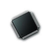
PIC18F87J72-I/PT Microchip Technology, PIC18F87J72-I/PT Datasheet - Page 434

PIC18F87J72-I/PT
Manufacturer Part Number
PIC18F87J72-I/PT
Description
IC PIC MCU 8BIT 14KB FLSH 80TQFP
Manufacturer
Microchip Technology
Series
PIC® 18Fr
Datasheet
1.PIC18F86J72-IPT.pdf
(480 pages)
Specifications of PIC18F87J72-I/PT
Program Memory Type
FLASH
Program Memory Size
128KB (64K x 16)
Package / Case
80-TQFP
Core Processor
PIC
Core Size
8-Bit
Speed
48MHz
Connectivity
I²C, LIN, SPI, UART/USART
Peripherals
Brown-out Detect/Reset, LCD, LVD, POR, PWM, WDT
Number Of I /o
51
Ram Size
3.8K x 8
Voltage - Supply (vcc/vdd)
2 V ~ 3.6 V
Data Converters
A/D 12x12b
Oscillator Type
Internal
Operating Temperature
-40°C ~ 85°C
Data Bus Width
8 bit
Data Ram Size
4 KB
Interface Type
SPI, USART, SPI, I2C
Maximum Clock Frequency
8 MHz
Number Of Programmable I/os
51
Number Of Timers
4
Operating Supply Voltage
2 V to 3.6 V
Maximum Operating Temperature
+ 85 C
Mounting Style
SMD/SMT
Minimum Operating Temperature
- 40 C
On-chip Adc
14
Controller Family/series
PIC18F
No. Of I/o's
51
Ram Memory Size
3923Byte
Cpu Speed
48MHz
No. Of Timers
4
Rohs Compliant
Yes
Lead Free Status / RoHS Status
Lead free / RoHS Compliant
Lead Free Status / RoHS Status
Lead free / RoHS Compliant, Lead free / RoHS Compliant
Available stocks
Company
Part Number
Manufacturer
Quantity
Price
Company:
Part Number:
PIC18F87J72-I/PT
Manufacturer:
Microchip
Quantity:
210
Company:
Part Number:
PIC18F87J72-I/PT
Manufacturer:
Microchip Technology
Quantity:
10 000
- Current page: 434 of 480
- Download datasheet (5Mb)
PIC18F87J72 FAMILY
APPENDIX B:
B.1
B.1.1
The dual-channel Analog Front End (AFE) contains two
synchronous sampling Delta-Sigma Analog-to-Digital
Converters (ADC), two PGAs, phase delay compensa-
tion block, internal voltage reference, modulator output
block and high-speed 20 MHz SPI compatible serial
interface. The converters contain a proprietary dithering
algorithm for reduced Idle tones and improved THD.
The internal register map contains 24-bit wide ADC
data words, as well as six writable control registers to
program gain, oversampling ratio, phase, resolution,
dithering,
features. The communication is largely simplified with
various continuous read modes that can be accessed
by the DMA of an external device, and with a separate
Data Ready (DR) pin that can directly be connected to
an IRQ input of an external microcontroller.
The AFE is capable of interfacing to a large variety of
voltage and current sensors, including shunts, current
transformers, Rogowski coils and Hall effect sensors.
B.1.2
The AFE incorporates two Delta-Sigma ADCs with a
multi-bit architecture. A Delta-Sigma ADC is an
oversampling converter that incorporates a built-in
modulator which is digitizing the quantity of charge
integrated by the modulator loop. The quantizer is the
block
conversion. The quantizer is typically 1-bit or a simple
comparator which helps to maintain the linearity
performance of the ADC (the DAC structure is in this
case inherently linear).
Multi-bit quantizers help to lower the quantization error
(the error fed back in the loop can be very large with
1-bit quantizers) without changing the order of the
modulator or the OSR which leads to better SNR
figures. However, typically, the linearity of such
architectures is more difficult to achieve since the DAC
is no more simple to realize and its linearity limits the
THD of such ADCs.
DS39979A-page 434
that
Introduction
DESCRIPTION
shutdown,
DELTA-SIGMA ADC
ARCHITECTURE
is
performing
DUAL-CHANNEL,
24-BIT AFE
REFERENCE
Reset
the
and
analog-to-digital
communication
Preliminary
The 5-level quantizer is a Flash ADC composed of
4 comparators, arranged with equally spaced thresh-
olds and a thermometer coding. The AFE also includes
proprietary, 5-level DAC architecture that is inherently
linear for improved THD figures.
B.1.3
• Two synchronous sampling 16/24-bit resolution
• 91 dB SINAD, -104 dBc THD (up to 35
• Programmable data rate of up to 64 ksps
• Ultra Low-Power Shutdown mode with <2 µA
• -133 dB crosstalk between the two channels
• Low drift internal voltage reference: 12 ppm/°C
• Differential voltage reference input pins
• High gain PGA on each channel (up to 32V/V)
• Phase delay compensation between the two
• Separate modulator outputs for each channel
• High-speed addressable 20 MHz SPI interface
• Independent analog and digital power supplies
• Low-power consumption (14 mW typical at 5V)
B.1.4
• Energy Metering and Power Measurement
• Automotive
• Portable Instrumentation
• Medical and Power Monitoring
Delta-Sigma A/D Converters with proprietary
multi-bit architecture
109 dB SFDR for each channel
channels with 1 µs time resolution
with Mode 0,0 and 1,1 compatibility
4.5V-5.5V SAV
FEATURES
APPLICATIONS
DD
, 2.7V-5.5V SV
2010 Microchip Technology Inc.
DD
th
harmonic),
Related parts for PIC18F87J72-I/PT
Image
Part Number
Description
Manufacturer
Datasheet
Request
R

Part Number:
Description:
Manufacturer:
Microchip Technology Inc.
Datasheet:

Part Number:
Description:
Manufacturer:
Microchip Technology Inc.
Datasheet:

Part Number:
Description:
Manufacturer:
Microchip Technology Inc.
Datasheet:

Part Number:
Description:
Manufacturer:
Microchip Technology Inc.
Datasheet:

Part Number:
Description:
Manufacturer:
Microchip Technology Inc.
Datasheet:

Part Number:
Description:
Manufacturer:
Microchip Technology Inc.
Datasheet:

Part Number:
Description:
Manufacturer:
Microchip Technology Inc.
Datasheet:

Part Number:
Description:
Manufacturer:
Microchip Technology Inc.
Datasheet:


