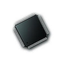
PIC18F87J72-I/PT Microchip Technology, PIC18F87J72-I/PT Datasheet - Page 422

PIC18F87J72-I/PT
Manufacturer Part Number
PIC18F87J72-I/PT
Description
IC PIC MCU 8BIT 14KB FLSH 80TQFP
Manufacturer
Microchip Technology
Series
PIC® 18Fr
Datasheet
1.PIC18F86J72-IPT.pdf
(480 pages)
Specifications of PIC18F87J72-I/PT
Program Memory Type
FLASH
Program Memory Size
128KB (64K x 16)
Package / Case
80-TQFP
Core Processor
PIC
Core Size
8-Bit
Speed
48MHz
Connectivity
I²C, LIN, SPI, UART/USART
Peripherals
Brown-out Detect/Reset, LCD, LVD, POR, PWM, WDT
Number Of I /o
51
Ram Size
3.8K x 8
Voltage - Supply (vcc/vdd)
2 V ~ 3.6 V
Data Converters
A/D 12x12b
Oscillator Type
Internal
Operating Temperature
-40°C ~ 85°C
Data Bus Width
8 bit
Data Ram Size
4 KB
Interface Type
SPI, USART, SPI, I2C
Maximum Clock Frequency
8 MHz
Number Of Programmable I/os
51
Number Of Timers
4
Operating Supply Voltage
2 V to 3.6 V
Maximum Operating Temperature
+ 85 C
Mounting Style
SMD/SMT
Minimum Operating Temperature
- 40 C
On-chip Adc
14
Controller Family/series
PIC18F
No. Of I/o's
51
Ram Memory Size
3923Byte
Cpu Speed
48MHz
No. Of Timers
4
Rohs Compliant
Yes
Lead Free Status / RoHS Status
Lead free / RoHS Compliant
Lead Free Status / RoHS Status
Lead free / RoHS Compliant, Lead free / RoHS Compliant
Available stocks
Company
Part Number
Manufacturer
Quantity
Price
Company:
Part Number:
PIC18F87J72-I/PT
Manufacturer:
Microchip
Quantity:
210
Company:
Part Number:
PIC18F87J72-I/PT
Manufacturer:
Microchip Technology
Quantity:
10 000
- Current page: 422 of 480
- Download datasheet (5Mb)
PIC18F87J72 FAMILY
FIGURE 29-19:
TABLE 29-25: A/D CONVERSION REQUIREMENTS
DS39979A-page 422
130
131
132
135
137
Note 1:
Param
No.
Note 1:
A/D CLK
A/D DATA
SAMPLE
2:
3:
4:
ADRES
BSF ADCON0, GO
T
T
T
T
T
Symbol
ADIF
AD
CNV
ACQ
SWC
DIS
2:
GO
Q4
The time of the A/D clock period is dependent on the device frequency and the T
ADRES registers may be read on the following T
The time for the holding capacitor to acquire the “New” input voltage when the voltage changes full scale
after the conversion (V
On the following cycle of the device clock.
(1)
If the A/D clock source is selected as RC, a time of T
to be executed.
This is a minimal RC delay (typically 100 ns), which also disconnects the holding capacitor from the analog input.
132
A/D Clock Period
Conversion Time
(not including acquisition time)
Acquisition Time
Switching Time from Convert Sample
Discharge Time
A/D CONVERSION TIMING
(Note 2)
Characteristic
DD
11
(3)
to V
10
SS
or V
OLD_DATA
9
SS
(2)
Preliminary
to V
. . .
SAMPLING STOPPED
CY
DD
is added before the A/D clock starts. This allows the SLEEP instruction
). The source impedance (R
CY
. . .
130
131
cycle.
Min
0.8
1.4
0.2
13
—
3
(Note 4)
12.5
Max
14
—
—
2
(1)
Units
1
T
s
s
s
AD
S
2010 Microchip Technology Inc.
) on the input channels is 50.
T
0
OSC
AD
based, V
clock divider.
NEW_DATA
DONE
Conditions
T
CY
REF
3.0V
Related parts for PIC18F87J72-I/PT
Image
Part Number
Description
Manufacturer
Datasheet
Request
R

Part Number:
Description:
Manufacturer:
Microchip Technology Inc.
Datasheet:

Part Number:
Description:
Manufacturer:
Microchip Technology Inc.
Datasheet:

Part Number:
Description:
Manufacturer:
Microchip Technology Inc.
Datasheet:

Part Number:
Description:
Manufacturer:
Microchip Technology Inc.
Datasheet:

Part Number:
Description:
Manufacturer:
Microchip Technology Inc.
Datasheet:

Part Number:
Description:
Manufacturer:
Microchip Technology Inc.
Datasheet:

Part Number:
Description:
Manufacturer:
Microchip Technology Inc.
Datasheet:

Part Number:
Description:
Manufacturer:
Microchip Technology Inc.
Datasheet:


