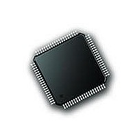
PIC18F87J72-I/PT Microchip Technology, PIC18F87J72-I/PT Datasheet - Page 69

PIC18F87J72-I/PT
Manufacturer Part Number
PIC18F87J72-I/PT
Description
IC PIC MCU 8BIT 14KB FLSH 80TQFP
Manufacturer
Microchip Technology
Series
PIC® 18Fr
Datasheet
1.PIC18F86J72-IPT.pdf
(480 pages)
Specifications of PIC18F87J72-I/PT
Program Memory Type
FLASH
Program Memory Size
128KB (64K x 16)
Package / Case
80-TQFP
Core Processor
PIC
Core Size
8-Bit
Speed
48MHz
Connectivity
I²C, LIN, SPI, UART/USART
Peripherals
Brown-out Detect/Reset, LCD, LVD, POR, PWM, WDT
Number Of I /o
51
Ram Size
3.8K x 8
Voltage - Supply (vcc/vdd)
2 V ~ 3.6 V
Data Converters
A/D 12x12b
Oscillator Type
Internal
Operating Temperature
-40°C ~ 85°C
Data Bus Width
8 bit
Data Ram Size
4 KB
Interface Type
SPI, USART, SPI, I2C
Maximum Clock Frequency
8 MHz
Number Of Programmable I/os
51
Number Of Timers
4
Operating Supply Voltage
2 V to 3.6 V
Maximum Operating Temperature
+ 85 C
Mounting Style
SMD/SMT
Minimum Operating Temperature
- 40 C
On-chip Adc
14
Controller Family/series
PIC18F
No. Of I/o's
51
Ram Memory Size
3923Byte
Cpu Speed
48MHz
No. Of Timers
4
Rohs Compliant
Yes
Lead Free Status / RoHS Status
Lead free / RoHS Compliant
Lead Free Status / RoHS Status
Lead free / RoHS Compliant, Lead free / RoHS Compliant
Available stocks
Company
Part Number
Manufacturer
Quantity
Price
Company:
Part Number:
PIC18F87J72-I/PT
Manufacturer:
Microchip
Quantity:
210
Company:
Part Number:
PIC18F87J72-I/PT
Manufacturer:
Microchip Technology
Quantity:
10 000
- Current page: 69 of 480
- Download datasheet (5Mb)
TABLE 6-3:
2010 Microchip Technology Inc.
SPBRGH1
BAUDCON1
LCDDATA22
LCDDATA21
LCDDATA20
LCDDATA19
LCDDATA18
LCDDATA16
LCDDATA15
LCDDATA14
LCDDATA13
LCDDATA12
LCDDATA10
LCDDATA9
LCDDATA8
LCDDATA7
LCDDATA6
CCPR1H
CCPR1L
CCP1CON
CCPR2H
CCPR2L
CCP2CON
SPBRG2
RCREG2
TXREG2
TXSTA2
RCSTA2
RTCCFG
RTCCAL
RTCVALH
RTCVALL
ALRMCFG
ALRMRPT
ALRMVALH
ALRMVALL
CTMUCONH
CTMUCONL
CTMUICON
PADCFG1
Legend:
Note 1:
File Name
2:
3:
4:
x = unknown, u = unchanged, - = unimplemented, q = value depends on condition, r = reserved, do not modify
Bit 21 of the PC is only available in Test mode and Serial Programming modes.
Alternate names and definitions for these bits when the MSSP module is operating in I
Masking” for details.
The PLLEN bit is only available in specific oscillator configurations; otherwise, it is disabled and reads as ‘0’. See Section 3.4.3 “PLL
Frequency Multiplier” for details.
RA<7:6> and their associated latch and direction bits are configured as port pins only when the internal oscillator is selected as the default
clock source (FOSC2 Configuration bit = 0); otherwise, they are disabled and these bits read as ‘0’.
EUSART Baud Rate Generator High Byte
Capture/Compare/PWM Register 1 High Byte
Capture/Compare/PWM Register 1 Low Byte
Capture/Compare/PWM Register 2 High Byte
Capture/Compare/PWM Register 2 Low Byte
AUSART Baud Rate Generator Register
AUSART Receive Register
AUSART Transmit Register
RTCC Value High Register Window based on RTCPTR<1:0>
RTCC Value Low Register Window based on RTCPTR<1:0>
Alarm Value High Register Window based on ALRMPTR<1:0>
Alarm Value Low Register Window based on ALRMPTR<1:0>
EDG2POL
ALRMEN
CTMUEN
ABDOVF
RTCEN
ARPT7
ITRIM5
S31C3
S23C3
S15C3
S07C3
S31C2
S23C2
S15C2
S07C2
S31C1
S23C1
S15C1
S07C1
CSRC
SPEN
CAL7
Bit 7
—
—
—
—
—
—
PIC18F87J72 FAMILY REGISTER FILE SUMMARY (CONTINUED)
EDG2SEL1 EDG2SEL0
ITRIM4
CHIME
ARPT6
S30C3
S22C3
S14C3
S06C3
S30C2
S22C2
S14C2
S06C2
S30C1
S22C1
S14C1
S06C1
RCMT
CAL6
Bit 6
RX9
TX9
—
—
—
—
—
—
—
—
RTCWREN
CTMUSIDL
AMASK3
RXDTP
DC1B1
DC2B1
ARPT5
ITRIM3
S29C3
S21C3
S13C3
S05C3
S29C2
S21C2
S13C2
S05C2
S29C1
S21C1
S13C1
S05C1
SREN
TXEN
CAL5
Bit 5
—
—
—
—
RTCSYNC
EDG1POL
AMASK2
TXCKP
DC1B0
DC2B0
ARPT4
ITRIM2
S28C3
S20C3
S12C3
S04C3
S28C2
S20C2
S12C2
S04C2
S28C1
S20C1
S12C1
S04C1
CREN
SYNC
TGEN
CAL4
Bit 4
—
—
—
—
Preliminary
EDG1SEL1 EDG1SEL0 EDG2STAT EDG1STAT 0000 0000
HALFSEC
CCP1M3
CCP2M3
AMASK1
ADDEN
EDGEN
BRG16
ARPT3
ITRIM1
S27C3
S19C3
S11C3
S03C3
S27C2
S19C2
S11C2
S03C2
S27C1
S19C1
S11C1
S03C1
CAL3
Bit 3
—
—
—
—
—
PIC18F87J72 FAMILY
RTSECSEL1 RTSECSEL0
EDGSEQEN
CCP1M2
CCP2M2
AMASK0
RTCOE
ITRIM0
ARPT2
S26C3
S18C3
S10C3
S02C3
S26C2
S18C2
S10C2
S02C2
S26C1
S18C1
S10C1
S02C1
BRGH
FERR
CAL2
Bit 2
—
—
—
—
2
C™ Slave mode. See Section 18.4.3.2 “Address
ALRMPTR1 ALRMPTR0 0000 0000
RTCPTR1
CCP1M1
CCP2M1
IDISSEN
ARPT1
S25C3
S17C3
S09C3
S01C3
S25C2
S17C2
S09C2
S01C2
S25C1
S17C1
S09C1
S01C1
OERR
IRNG1
TRMT
CAL1
WUE
Bit 1
—
—
—
RTCPTR0
CCP1M0
CCP2M0
CTTRIG
ABDEN
ARPT0
S32C3
S24C3
S16C3
S08C3
S00C3
S32C2
S24C2
S16C2
S08C2
S00C2
S32C1
S24C1
S16C1
S08C1
S00C1
IRNG0
RX9D
TX9D
CAL0
Bit 0
—
0000 0000
0100 0-00
xxxx xxxx
xxxx xxxx
xxxx xxxx
xxxx xxxx
xxxx xxxx
xxxx xxxx
xxxx xxxx
xxxx xxxx
xxxx xxxx
xxxx xxxx
xxxx xxxx
xxxx xxxx
xxxx xxxx
xxxx xxxx
xxxx xxxx
xxxx xxxx
xxxx xxxx
--00 0000
xxxx xxxx
xxxx xxxx
--00 0000
0000 0000
0000 0000
0000 0000
0000 -010
0000 000x
0-00 0000
0000 0000
xxxx xxxx
xxxx xxxx
0000 0000
xxxx xxxx
xxxx xxxx
0-00 0000
0000 0000
---- -00-
POR, BOR
DS39979A-page 69
Value on
Details on
53, 243
53, 242
53, 171
53, 171
53, 171
53, 171
53, 171
53, 171
53, 171
53, 171
53, 171
53, 171
53, 171
53, 171
53, 171
53, 171
53, 171
53, 158
53, 158
53, 157
53, 158
53, 158
53, 157
54, 262
54, 267
54, 265
54, 260
54, 261
54, 141
54, 142
54, 144
54, 144
54, 143
54, 144
54, 147
54, 147
54, 315
54, 316
54, 317
54, 142
page
Related parts for PIC18F87J72-I/PT
Image
Part Number
Description
Manufacturer
Datasheet
Request
R

Part Number:
Description:
Manufacturer:
Microchip Technology Inc.
Datasheet:

Part Number:
Description:
Manufacturer:
Microchip Technology Inc.
Datasheet:

Part Number:
Description:
Manufacturer:
Microchip Technology Inc.
Datasheet:

Part Number:
Description:
Manufacturer:
Microchip Technology Inc.
Datasheet:

Part Number:
Description:
Manufacturer:
Microchip Technology Inc.
Datasheet:

Part Number:
Description:
Manufacturer:
Microchip Technology Inc.
Datasheet:

Part Number:
Description:
Manufacturer:
Microchip Technology Inc.
Datasheet:

Part Number:
Description:
Manufacturer:
Microchip Technology Inc.
Datasheet:


