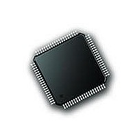
PIC18F87J72-I/PT Microchip Technology, PIC18F87J72-I/PT Datasheet - Page 285

PIC18F87J72-I/PT
Manufacturer Part Number
PIC18F87J72-I/PT
Description
IC PIC MCU 8BIT 14KB FLSH 80TQFP
Manufacturer
Microchip Technology
Series
PIC® 18Fr
Datasheet
1.PIC18F86J72-IPT.pdf
(480 pages)
Specifications of PIC18F87J72-I/PT
Program Memory Type
FLASH
Program Memory Size
128KB (64K x 16)
Package / Case
80-TQFP
Core Processor
PIC
Core Size
8-Bit
Speed
48MHz
Connectivity
I²C, LIN, SPI, UART/USART
Peripherals
Brown-out Detect/Reset, LCD, LVD, POR, PWM, WDT
Number Of I /o
51
Ram Size
3.8K x 8
Voltage - Supply (vcc/vdd)
2 V ~ 3.6 V
Data Converters
A/D 12x12b
Oscillator Type
Internal
Operating Temperature
-40°C ~ 85°C
Data Bus Width
8 bit
Data Ram Size
4 KB
Interface Type
SPI, USART, SPI, I2C
Maximum Clock Frequency
8 MHz
Number Of Programmable I/os
51
Number Of Timers
4
Operating Supply Voltage
2 V to 3.6 V
Maximum Operating Temperature
+ 85 C
Mounting Style
SMD/SMT
Minimum Operating Temperature
- 40 C
On-chip Adc
14
Controller Family/series
PIC18F
No. Of I/o's
51
Ram Memory Size
3923Byte
Cpu Speed
48MHz
No. Of Timers
4
Rohs Compliant
Yes
Lead Free Status / RoHS Status
Lead free / RoHS Compliant
Lead Free Status / RoHS Status
Lead free / RoHS Compliant, Lead free / RoHS Compliant
Available stocks
Company
Part Number
Manufacturer
Quantity
Price
Company:
Part Number:
PIC18F87J72-I/PT
Manufacturer:
Microchip
Quantity:
210
Company:
Part Number:
PIC18F87J72-I/PT
Manufacturer:
Microchip Technology
Quantity:
10 000
- Current page: 285 of 480
- Download datasheet (5Mb)
22.2
The dual-channel AFE uses its own internal registers
for data and control. This memory is not mapped to the
microcontroller’s SFR space, but is accessed through
the AFE’s serial interface. The memory space is
divided into eight registers:
• Two 24-bit registers, one for the data of each ADC
• Five 8-bit control registers
• One reserved 8-bit register address
Although the data registers are 24 bits wide, they may
be directly addressed as three different 8-bit registers.
The complete memory map is listed in Table 22-1.
.
TABLE 22-1:
TABLE 22-2:
2010 Microchip Technology Inc.
DATA_CH0
DATA_CH1
PHASE
GAIN
STATUS/COM
CONFIG1
CONFIG2
Address
0Ah
0Bh
00h
03h
06h
07h
08h
09h
Function
AFE Register Map
STATUS/COM
DATA_CH0
DATA_CH1
REGISTER MAP GROUPING FOR CONTINUOUS READ MODES
CONFIG1
CONFIG2
Reserved
AFE REGISTER MAP
PHASE
Name
GAIN
Address
0Ah
0Bh
00h
01h
02h
03h
04h
05h
07h
08h
09h
Bits
24
24
8
8
8
8
8
8
R/W
R/W Phase Delay Configuration Register
R/W Gain Configuration Register
R/W Status/Communication Register
R/W Configuration Register 1
R/W Configuration Register 2
—
R
R
Channel 0 ADC Data <23:0>, MSB First
Channel 1 ADC Data <23:0>, MSB First
Reserved; ignore reads, do not write
Preliminary
Group
Group
Group
Group
“01”
PIC18F87J72 FAMILY
All registers are fully described in Section B.6 “Internal
Registers” of the AFE reference.
Registers may be read singly in a single read opera-
tion; continuously, as part of a group of registers; or
continuously, by type (i.e., data registers vs. control
registers). The type of read operation is handled
through the AFE’s serial interface by selecting the type
of read operation. The grouping of registers is shown in
Table 22-2. A complete description of the different read
operations and how to implement them is described in
Section B.5.3 “Reading from the Device” of the AFE
reference.
READ<1:0>
Description
“10”
Type
Type
DS39979A-page 285
Register Map
Loop Entire
“11”
Related parts for PIC18F87J72-I/PT
Image
Part Number
Description
Manufacturer
Datasheet
Request
R

Part Number:
Description:
Manufacturer:
Microchip Technology Inc.
Datasheet:

Part Number:
Description:
Manufacturer:
Microchip Technology Inc.
Datasheet:

Part Number:
Description:
Manufacturer:
Microchip Technology Inc.
Datasheet:

Part Number:
Description:
Manufacturer:
Microchip Technology Inc.
Datasheet:

Part Number:
Description:
Manufacturer:
Microchip Technology Inc.
Datasheet:

Part Number:
Description:
Manufacturer:
Microchip Technology Inc.
Datasheet:

Part Number:
Description:
Manufacturer:
Microchip Technology Inc.
Datasheet:

Part Number:
Description:
Manufacturer:
Microchip Technology Inc.
Datasheet:


