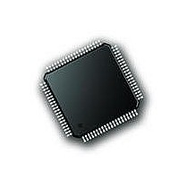
PIC18F87J72-I/PT Microchip Technology, PIC18F87J72-I/PT Datasheet - Page 83

PIC18F87J72-I/PT
Manufacturer Part Number
PIC18F87J72-I/PT
Description
IC PIC MCU 8BIT 14KB FLSH 80TQFP
Manufacturer
Microchip Technology
Series
PIC® 18Fr
Datasheet
1.PIC18F86J72-IPT.pdf
(480 pages)
Specifications of PIC18F87J72-I/PT
Program Memory Type
FLASH
Program Memory Size
128KB (64K x 16)
Package / Case
80-TQFP
Core Processor
PIC
Core Size
8-Bit
Speed
48MHz
Connectivity
I²C, LIN, SPI, UART/USART
Peripherals
Brown-out Detect/Reset, LCD, LVD, POR, PWM, WDT
Number Of I /o
51
Ram Size
3.8K x 8
Voltage - Supply (vcc/vdd)
2 V ~ 3.6 V
Data Converters
A/D 12x12b
Oscillator Type
Internal
Operating Temperature
-40°C ~ 85°C
Data Bus Width
8 bit
Data Ram Size
4 KB
Interface Type
SPI, USART, SPI, I2C
Maximum Clock Frequency
8 MHz
Number Of Programmable I/os
51
Number Of Timers
4
Operating Supply Voltage
2 V to 3.6 V
Maximum Operating Temperature
+ 85 C
Mounting Style
SMD/SMT
Minimum Operating Temperature
- 40 C
On-chip Adc
14
Controller Family/series
PIC18F
No. Of I/o's
51
Ram Memory Size
3923Byte
Cpu Speed
48MHz
No. Of Timers
4
Rohs Compliant
Yes
Lead Free Status / RoHS Status
Lead free / RoHS Compliant
Lead Free Status / RoHS Status
Lead free / RoHS Compliant, Lead free / RoHS Compliant
Available stocks
Company
Part Number
Manufacturer
Quantity
Price
Company:
Part Number:
PIC18F87J72-I/PT
Manufacturer:
Microchip
Quantity:
210
Company:
Part Number:
PIC18F87J72-I/PT
Manufacturer:
Microchip Technology
Quantity:
10 000
- Current page: 83 of 480
- Download datasheet (5Mb)
7.5
The programming block is 32 words or 64 bytes.
Programming one word or two bytes at a time is also
supported.
Table writes are used internally to load the holding
registers needed to program the Flash memory. There
are 64 holding registers used by the table writes for
programming.
Since the Table Latch (TABLAT) is only a single byte, the
TBLWT instruction may need to be executed 64 times for
each programming operation (if WPROG = 0). All of the
table write operations will essentially be short writes
because only the holding registers are written. At the
end of updating the 64 holding registers, the EECON1
register must be written to in order to start the
programming operation with a long write.
The long write is necessary for programming the inter-
nal Flash. Instruction execution is halted while in a long
write cycle. The long write will be terminated by the
internal programming timer.
FIGURE 7-5:
7.5.1
The sequence of events for programming an internal
program memory location should be:
1.
2.
3.
4.
5.
6.
7.
2010 Microchip Technology Inc.
TBLPTR = xxxxx0
Read 1,024 bytes into RAM.
Update data values in RAM as necessary.
Load Table Pointer register with the address
being erased.
Execute the erase procedure.
Load Table Pointer register with the address of
the first byte being written, minus 1.
Write the 64 bytes into the holding registers with
auto-increment.
Set the WREN bit (EECON1<2>) to enable byte
writes.
Writing to Flash Program Memory
FLASH PROGRAM MEMORY WRITE
SEQUENCE
Holding Register
TABLE WRITES TO FLASH PROGRAM MEMORY
8
TBLPTR = xxxxx1
Holding Register
8
Preliminary
Program Memory
TBLPTR = xxxxx2
Write Register
TABLAT
PIC18F87J72 FAMILY
The on-chip timer controls the write time. The
write/erase voltages are generated by an on-chip
charge pump, rated to operate over the voltage range
of the device.
8.
9.
10. Write 0AAh to EECON2.
11. Set the WR bit. This will begin the write cycle.
12. The CPU will stall for the duration of the write for
13. Re-enable interrupts.
14. Repeat steps 6 through 13 until all 1,024 bytes
15. Verify the memory (table read).
An example of the required code is shown in
Example 7-3 on the following page.
Note:
Holding Register
Note 1: Unlike previous PIC18 Flash devices,
Disable interrupts.
Write 55h to EECON2.
T
are written to program memory.
IW
(parameter D133A).
2: To maintain the endurance of the program
8
Before setting the WR bit, the Table
Pointer address needs to be within the
intended address range of the 64 bytes in
the holding register.
members of the PIC18F87J72 family do
not reset the holding registers after a
write occurs. The holding registers must
be cleared or overwritten before a
programming sequence.
memory cells, each Flash byte should not
be programmed more than one time
between
attempting to modify the contents of the
target cell a second time, an erase of the
target, or a bulk erase of the entire
memory, must be performed.
erase
TBLPTR = xxxx3F
operations.
Holding Register
DS39979A-page 83
8
Before
Related parts for PIC18F87J72-I/PT
Image
Part Number
Description
Manufacturer
Datasheet
Request
R

Part Number:
Description:
Manufacturer:
Microchip Technology Inc.
Datasheet:

Part Number:
Description:
Manufacturer:
Microchip Technology Inc.
Datasheet:

Part Number:
Description:
Manufacturer:
Microchip Technology Inc.
Datasheet:

Part Number:
Description:
Manufacturer:
Microchip Technology Inc.
Datasheet:

Part Number:
Description:
Manufacturer:
Microchip Technology Inc.
Datasheet:

Part Number:
Description:
Manufacturer:
Microchip Technology Inc.
Datasheet:

Part Number:
Description:
Manufacturer:
Microchip Technology Inc.
Datasheet:

Part Number:
Description:
Manufacturer:
Microchip Technology Inc.
Datasheet:


