IPR-RLDII/UNI Altera, IPR-RLDII/UNI Datasheet - Page 31
IPR-RLDII/UNI
Manufacturer Part Number
IPR-RLDII/UNI
Description
IP CORE Renewal Of IP-RLDII/UNI
Manufacturer
Altera
Datasheet
1.IP-RLDIIUNI.pdf
(76 pages)
Specifications of IPR-RLDII/UNI
Software Application
IP CORE, Memory Controllers, SDRAM
Supported Families
Arria II GZ, Stratix III, Stratix IV, HardCopy III
Core Architecture
FPGA
Core Sub-architecture
Arria, HardCopy, Stratix
Rohs Compliant
NA
Lead Free Status / RoHS Status
na


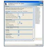
Chapter 3: Parameter Settings
Memory Parameters
Memory Parameters
Memory Timing
December 2010 Altera Corporation
The Memory Parameters tab allows you to configure memory device parameters. You
can enter parameters manually from the manufacturer’s device data sheet, or you can
populate the fields automatically by selecting the required device from the list of
presets.
Table 3–5
Table 3–5. Memory Parameters
The Memory Timing tab allows you to configure memory device timing parameters.
You can enter timing parameters manually from the manufacturer’s device data
sheet, or you can populate the fields automatically by selecting the required device
from the list of presets.
Table 3–6
Table 3–6. Memory Timing Parameters (Part 1 of 2)
Address width
Data width
Bank-address width
Data-mask width
QK width
DK width
Burst length
Memory mode register configuration
Maximum memory clock frequency
Refresh interval
tCKH (%)
tQKH (%)
tAS
tAH
tDS
tDH
tQKQ_max
tQKQ_min
describes the memory parameters.
describes the memory timing parameters.
Parameters
Parameter
The width of the address bus on the memory device.
The width of the data bus on the memory device.
The width of the bank-address bus on the memory device.
The width of the data-mask on the memory device,
The width of the QK (read strobe) bus on the memory
device.
The width of the DK (write strobe) bus on the memory
device.
The burst length supported by the memory device.
Configuration bits that set the memory mode.
The maximum frequency at which the memory device can
run.
The refresh interval.
The input clock (K/K#) high expressed as a percentage of
the full clock period.
The read clock (QK/QK#) high expressed as a percentage of
tCKH.
Address and control setup to K clock rise.
Address and control hold after K clock rise.
Data setup to clock (K/K#) rise.
Data hold after clock (K/K#) rise.
QK clock edge to DQ data edge (in same group).
QK clock edge to DQ data edge (in same group).
Section IV. RLDRAM II Controller with UniPHY IP User Guide
External Memory Interface Handbook Volume 3
Description
Description
3–3
Related parts for IPR-RLDII/UNI
Image
Part Number
Description
Manufacturer
Datasheet
Request
R

Part Number:
Description:
IP CORE Renewal Of IP-XAUIPCS
Manufacturer:
Altera
Datasheet:

Part Number:
Description:
CYCLONE II STARTER KIT EP2C20N
Manufacturer:
Altera
Datasheet:

Part Number:
Description:
CPLD, EP610 Family, ECMOS Process, 300 Gates, 16 Macro Cells, 16 Reg., 16 User I/Os, 5V Supply, 35 Speed Grade, 24DIP
Manufacturer:
Altera Corporation
Datasheet:
Part Number:
Description:
CPLD, EP610 Family, ECMOS Process, 300 Gates, 16 Macro Cells, 16 Reg., 16 User I/Os, 5V Supply, 15 Speed Grade, 24DIP
Manufacturer:
Altera Corporation
Datasheet:
Part Number:
Description:
Manufacturer:
Altera Corporation
Datasheet:
Part Number:
Description:
CPLD, EP610 Family, ECMOS Process, 300 Gates, 16 Macro Cells, 16 Reg., 16 User I/Os, 5V Supply, 30 Speed Grade, 24DIP
Manufacturer:
Altera Corporation
Datasheet:
Part Number:
Description:
High-performance, low-power erasable programmable logic devices with 8 macrocells, 10ns
Manufacturer:
Altera Corporation
Datasheet:
Part Number:
Description:
High-performance, low-power erasable programmable logic devices with 8 macrocells, 7ns
Manufacturer:
Altera Corporation
Datasheet:
Part Number:
Description:
Classic EPLD
Manufacturer:
Altera Corporation
Datasheet:
Part Number:
Description:
High-performance, low-power erasable programmable logic devices with 8 macrocells, 10ns
Manufacturer:
Altera Corporation
Datasheet:
Part Number:
Description:
Manufacturer:
Altera Corporation
Datasheet:
Part Number:
Description:
Manufacturer:
Altera Corporation
Datasheet: