IPR-RLDII/UNI Altera, IPR-RLDII/UNI Datasheet - Page 35
IPR-RLDII/UNI
Manufacturer Part Number
IPR-RLDII/UNI
Description
IP CORE Renewal Of IP-RLDII/UNI
Manufacturer
Altera
Datasheet
1.IP-RLDIIUNI.pdf
(76 pages)
Specifications of IPR-RLDII/UNI
Software Application
IP CORE, Memory Controllers, SDRAM
Supported Families
Arria II GZ, Stratix III, Stratix IV, HardCopy III
Core Architecture
FPGA
Core Sub-architecture
Arria, HardCopy, Stratix
Rohs Compliant
NA
Lead Free Status / RoHS Status
na


Add Pin and DQ Group Assignments
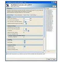
Board Settings Tab
December 2010 Altera Corporation
f
1
The Quartus II software generates a Synopsis Design Constraint (.sdc) script,
<variation_name>.sdc, and a pin assignment script,
<variation_name>_pin_assignments.tcl. Both the .sdc and the <variation
name>_pin_assignments.tcl support multiple instances. These scripts iterate through
all instances of the core and apply the same constraints to all of them.
The pin assignment script, <variation_name>_pin_assignments.tcl, sets up the I/O
standards and the input/output termination for the RLDRAM II controller with
UniPHY. This script also helps to relate the DQ and QK pin groups together for the
Fitter to place them correctly.
The pin assignment script does not create a source clock for the design. You must
create a clock for the design and provide pin assignments for the signals of both the
example driver and testbench that the MegaCore variation generates.
Run the <variation_name>_pin_assignments.tcl to add the input and output
termination, I/O standards, and DQ group assignments to the example design. To
run the pin assignment script, follow these steps:
1. On Processing menu, point to Start, and click Start Analysis and Synthesis.
2. On the Tools menu click Tcl Scripts.
3. Specify the <variation_name>_pin_assignments.tcl file and click Run.
If the PLL input reference clock pin is not the same I/O standard as the memory
interface I/Os, the design might not fit into the device because incompatible I/O
standards cannot be placed in the same I/O bank.
The Board Settings tab allows you to enter board-related data. In the Setup and Hold
Derating section, you enter derating parameters from the device data sheet, which the
system uses to calculate derated setup and hold values. In the Intersymbol
Interference and Board Skews sections, you enter information derived during your
PCB development process of prelayout (line) simulation and finally postlayout
(board) simulation.
Timing analysis does not consider bus turnaround; consequently, the controller dead
times are based on assumptions about the user board trace lengths. For timing
analysis to be accurate, board trace delays must not exceed 0.6 ns from FPGA to
memory and from memory to FPGA.
For more information about how to include your board simulation results in the
Quartus II software and how to assign pins using pin planners, refer to
Design Flow Tutorials
of the External Memory Interface Handbook.
4. Constraining and Compiling
Section IV. RLDRAM II Controller with UniPHY IP User Guide
External Memory Interface Handbook Volume 3
Volume 6:
Related parts for IPR-RLDII/UNI
Image
Part Number
Description
Manufacturer
Datasheet
Request
R

Part Number:
Description:
IP CORE Renewal Of IP-XAUIPCS
Manufacturer:
Altera
Datasheet:

Part Number:
Description:
CYCLONE II STARTER KIT EP2C20N
Manufacturer:
Altera
Datasheet:

Part Number:
Description:
CPLD, EP610 Family, ECMOS Process, 300 Gates, 16 Macro Cells, 16 Reg., 16 User I/Os, 5V Supply, 35 Speed Grade, 24DIP
Manufacturer:
Altera Corporation
Datasheet:
Part Number:
Description:
CPLD, EP610 Family, ECMOS Process, 300 Gates, 16 Macro Cells, 16 Reg., 16 User I/Os, 5V Supply, 15 Speed Grade, 24DIP
Manufacturer:
Altera Corporation
Datasheet:
Part Number:
Description:
Manufacturer:
Altera Corporation
Datasheet:
Part Number:
Description:
CPLD, EP610 Family, ECMOS Process, 300 Gates, 16 Macro Cells, 16 Reg., 16 User I/Os, 5V Supply, 30 Speed Grade, 24DIP
Manufacturer:
Altera Corporation
Datasheet:
Part Number:
Description:
High-performance, low-power erasable programmable logic devices with 8 macrocells, 10ns
Manufacturer:
Altera Corporation
Datasheet:
Part Number:
Description:
High-performance, low-power erasable programmable logic devices with 8 macrocells, 7ns
Manufacturer:
Altera Corporation
Datasheet:
Part Number:
Description:
Classic EPLD
Manufacturer:
Altera Corporation
Datasheet:
Part Number:
Description:
High-performance, low-power erasable programmable logic devices with 8 macrocells, 10ns
Manufacturer:
Altera Corporation
Datasheet:
Part Number:
Description:
Manufacturer:
Altera Corporation
Datasheet:
Part Number:
Description:
Manufacturer:
Altera Corporation
Datasheet: