CDB42L55 Cirrus Logic Inc, CDB42L55 Datasheet - Page 15
CDB42L55
Manufacturer Part Number
CDB42L55
Description
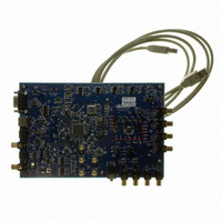
Eval Bd Ultra Low Power Stereo Codec
Manufacturer
Cirrus Logic Inc
Specifications of CDB42L55
Main Purpose
Audio, CODEC
Embedded
Yes, FPGA / CPLD
Utilized Ic / Part
CS42L55
Primary Attributes
2 Stereo Analog Inputs, Stereo Line and Headphone Outputs, S/PDIF Transmitter and Receiver
Secondary Attributes
GUI, USB, RS232, I2C Interfaces, USB or External or Battery Power Supply
Product
Audio Modules
Lead Free Status / RoHS Status
Contains lead / RoHS non-compliant
Lead Free Status / RoHS Status
Contains lead / RoHS non-compliant
Other names
598-1506
CDB-42L55
CDB-42L55


DS773F1
LINE OUTPUT CHARACTERISTICS
Test conditions (unless otherwise specified): Connections to the CS42L55 are shown in the
page
Measurement bandwidth is 20 Hz to 20 kHz; Sample Frequency = 48 kHz; Test load R
page
Notes:
Parameter
Dynamic Range
18 to 24-Bit
16-Bit
Total Harmonic Distortion + Noise
18 to 24-Bit
16-Bit
Full-scale Output Voltage
Other Characteristics
Interchannel Isolation
Interchannel Gain Mismatch
Output Offset Voltage
Gain Drift
Output Impedance
AC-Load Resistance (R
Load Capacitance (C
(+2 dB Analog Gain)
10; Input test signal is a full-scale 997 Hz sine wave; All Supplies = VA, VCP Mode; GND = AGND = 0 V; T
15).
Figure 3. HP Output Test Configuration
11. One-half LSB of triangular PDF dither is added to data.
12. The Analog Gain setting (refer to
13. VCP settings lower than VA reduces the headroom of the headphone amplifier. As a result, the speci-
14. See
GND/AGND
HPOUTx
page
tings at certain VA and VCP supply levels may cause clipping when the audio signal approaches full-
scale, maximum power output.
fied THD+N performance at full-scale output voltage and power may not be achieved.
(Note 11)
HPREF
Figure 3
58) must be configured as indicated to achieve the specified output characteristics. High gain set-
0.1 μF
33 Ω
L
(Note 14)
)
(Note 12)
L
)
(Note 13)
C
and
L
=150 pF
Test Load
Figure 4 on page
R
3 k
L
DAC to LINEOUT
=16
Ω
Measurement
Ω
-
Device
or
unweighted
unweighted
A-weighted
A-weighted
+
(Note 14)
(Note 14)
-20 dB
-60 dB
-20 dB
-60 dB
“Headphone Volume Control” on page 57
0 dB
0 dB
15. Refer to
1.50•VA
Min
93
90
3
-
-
-
-
-
-
-
-
-
-
-
-
-
-
VA = 2.5 V
“Parameter Definitions” on page
1.58•VA
Figure 4. Line Output Test Configuration
±100
Typ
100
-84
-76
-36
-82
-74
-34
0.1
0.5
99
96
96
93
90
-
-
G N D /A G N D
LIN E O U Tx
1.66•VA 1.50•VA 1.58•VA 1.66•VA
LIN E R E F
Max
0.25
150
-78
-30
1.0
-
-
-
-
-
-
-
-
-
-
-
-
L
= 3 kΩ, C
Min
91
88
“Typical Connection Diagram” on
3
-
-
-
-
-
-
-
-
-
-
-
-
-
-
C
VA = 1.8 V
or
L
=150 pF
L
T est Load
= 150 pF (see
“Line Volume Control” on
±100
Typ
100
-86
-74
-34
-84
-72
-32
0.1
0.2
97
94
94
91
90
-
-
71.
R
L
=3 k
M easurem ent
Ω
-
D evice
Max
0.25
150
-80
-28
1.0
-
-
-
-
-
-
-
-
-
-
-
-
CS42L55
A
Figure 3 on
= +25 °C;
+
ppm/°C
Unit
V
mV
dB
dB
dB
dB
dB
dB
dB
dB
dB
dB
dB
dB
kΩ
pF
Ω
PP
15
Related parts for CDB42L55
Image
Part Number
Description
Manufacturer
Datasheet
Request
R

Part Number:
Description:
Development Kit
Manufacturer:
Cirrus Logic Inc
Datasheet:
Part Number:
Description:
Development Kit
Manufacturer:
Cirrus Logic Inc
Datasheet:


Part Number:
Description:
High-efficiency PFC + Fluorescent Lamp Driver Reference Design
Manufacturer:
Cirrus Logic Inc
Datasheet:
Part Number:
Description:
Development Kit
Manufacturer:
Cirrus Logic Inc
Datasheet:
Part Number:
Description:
Development Kit
Manufacturer:
Cirrus Logic Inc
Datasheet:

Part Number:
Description:
Development Kit
Manufacturer:
Cirrus Logic Inc
Datasheet:
Part Number:
Description:
Development Kit
Manufacturer:
Cirrus Logic Inc
Datasheet:
Part Number:
Description:
Development Kit
Manufacturer:
Cirrus Logic Inc
Datasheet:
Part Number:
Description:
Development Kit
Manufacturer:
Cirrus Logic Inc
Datasheet:

Part Number:
Description:
EVALUATION BOARD FOR CS8427
Manufacturer:
Cirrus Logic Inc
Datasheet:

Part Number:
Description:
BOARD EVAL FOR CS8416 RCVR
Manufacturer:
Cirrus Logic Inc
Datasheet:

Part Number:
Description:
EVALUATION BOARD FOR CS8420
Manufacturer:
Cirrus Logic Inc
Datasheet:

Part Number:
Description:
KIT DEVELOPMENT EP9315 ARM9
Manufacturer:
Cirrus Logic Inc
Datasheet:

Part Number:
Description:
KIT DEVELOPMENT EP9302 ARM9
Manufacturer:
Cirrus Logic Inc
Datasheet: