CDB42L55 Cirrus Logic Inc, CDB42L55 Datasheet - Page 3
CDB42L55
Manufacturer Part Number
CDB42L55
Description
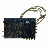
Eval Bd Ultra Low Power Stereo Codec
Manufacturer
Cirrus Logic Inc
Specifications of CDB42L55
Main Purpose
Audio, CODEC
Embedded
Yes, FPGA / CPLD
Utilized Ic / Part
CS42L55
Primary Attributes
2 Stereo Analog Inputs, Stereo Line and Headphone Outputs, S/PDIF Transmitter and Receiver
Secondary Attributes
GUI, USB, RS232, I2C Interfaces, USB or External or Battery Power Supply
Product
Audio Modules
Lead Free Status / RoHS Status
Contains lead / RoHS non-compliant
Lead Free Status / RoHS Status
Contains lead / RoHS non-compliant
Other names
598-1506
CDB-42L55
CDB-42L55


DS773F1
TABLE OF CONTENTS
1. PIN DESCRIPTIONS .............................................................................................................................. 8
2. TYPICAL CONNECTION DIAGRAM ................................................................................................... 10
3. CHARACTERISTIC AND SPECIFICATION TABLES ......................................................................... 11
4. APPLICATIONS ................................................................................................................................... 22
RECOMMENDED OPERATING CONDITIONS ................................................................................... 11
ABSOLUTE MAXIMUM RATINGS ....................................................................................................... 11
ANALOG INPUT CHARACTERISTICS ................................................................................................ 12
ADC DIGITAL FILTER CHARACTERISTICS ....................................................................................... 13
HP OUTPUT CHARACTERISTICS ...................................................................................................... 14
LINE OUTPUT CHARACTERISTICS ................................................................................................... 15
ANALOG PASSTHROUGH CHARACTERISTICS ............................................................................... 16
COMBINED DAC INTERPOLATION & ON-CHIP ANALOG FILTER RESPONSE .............................. 16
SWITCHING SPECIFICATIONS - SERIAL PORT ............................................................................... 17
SWITCHING SPECIFICATIONS - CONTROL PORT .......................................................................... 18
POWER SUPPLY REJECTION (PSRR) CHARACTERISTICS ........................................................... 19
DIGITAL INTERFACE SPECIFICATIONS & CHARACTERISTICS ..................................................... 19
POWER CONSUMPTION - ALL SUPPLIES = 1.8 V ............................................................................ 20
POWER CONSUMPTION - ALL SUPPLIES = 2.5 V ............................................................................ 21
1.1 I/O Pin Characteristics ...................................................................................................................... 9
4.1 Overview ......................................................................................................................................... 22
4.2 Analog Inputs ................................................................................................................................. 23
4.3 Analog In to Analog Out Passthrough ............................................................................................ 25
4.4 Analog Outputs .............................................................................................................................. 26
4.5 Class H Amplifier ............................................................................................................................ 27
4.6 Beep Generator .............................................................................................................................. 31
4.7 Limiter ............................................................................................................................................. 32
4.8 Serial Port Clocking ........................................................................................................................ 34
4.9 Digital Interface Format .................................................................................................................. 34
4.10 Initialization ................................................................................................................................... 34
4.11 Recommended DAC to HP or Line Power-Up Sequence (Playback) .......................................... 35
4.12 Recommended PGA to HP or Line Power-Up Sequence (Analog Passthrough) ......................... 36
4.13 Required Initialization Settings ..................................................................................................... 37
4.14 Control Port Operation .................................................................................................................. 38
4.1.1 Basic Architecture ................................................................................................................. 22
4.1.2 Line Inputs ............................................................................................................................. 22
4.1.3 Line and Headphone Outputs (Class H, Ground-Centered Amplifiers) ................................. 22
4.1.4 Fixed-Function DSP Engine .................................................................................................. 22
4.1.5 Beep Generator ..................................................................................................................... 22
4.1.6 Power Management .............................................................................................................. 22
4.2.1 Pseudo-Differential Inputs ..................................................................................................... 24
4.2.2 Automatic Level Control (ALC) .............................................................................................. 24
4.5.1 Power Control Options .......................................................................................................... 27
4.5.2 Power Supply Transitions ...................................................................................................... 29
4.5.3 Efficiency ............................................................................................................................... 31
4.11.1 Recommended Power-Down Sequence ............................................................................. 36
4.12.1 Recommended Power-Down Sequence ............................................................................. 36
4.14.1 I²C Control ........................................................................................................................... 38
4.14.2 Memory Address Pointer (MAP) .......................................................................................... 39
4.5.1.1 Standard Class AB Operation (Mode 01 and 10) ...................................................... 28
4.5.1.2 Adapted to Volume Settings (Mode 00) ..................................................................... 28
4.5.1.3 Adapted to Output Signal (Mode 11) ......................................................................... 29
4.14.2.1 Map Increment (INCR) ............................................................................................. 39
CS42L55
3
Related parts for CDB42L55
Image
Part Number
Description
Manufacturer
Datasheet
Request
R

Part Number:
Description:
Development Kit
Manufacturer:
Cirrus Logic Inc
Datasheet:
Part Number:
Description:
Development Kit
Manufacturer:
Cirrus Logic Inc
Datasheet:


Part Number:
Description:
High-efficiency PFC + Fluorescent Lamp Driver Reference Design
Manufacturer:
Cirrus Logic Inc
Datasheet:
Part Number:
Description:
Development Kit
Manufacturer:
Cirrus Logic Inc
Datasheet:
Part Number:
Description:
Development Kit
Manufacturer:
Cirrus Logic Inc
Datasheet:

Part Number:
Description:
Development Kit
Manufacturer:
Cirrus Logic Inc
Datasheet:
Part Number:
Description:
Development Kit
Manufacturer:
Cirrus Logic Inc
Datasheet:
Part Number:
Description:
Development Kit
Manufacturer:
Cirrus Logic Inc
Datasheet:
Part Number:
Description:
Development Kit
Manufacturer:
Cirrus Logic Inc
Datasheet:

Part Number:
Description:
EVALUATION BOARD FOR CS8427
Manufacturer:
Cirrus Logic Inc
Datasheet:

Part Number:
Description:
BOARD EVAL FOR CS8416 RCVR
Manufacturer:
Cirrus Logic Inc
Datasheet:

Part Number:
Description:
EVALUATION BOARD FOR CS8420
Manufacturer:
Cirrus Logic Inc
Datasheet:

Part Number:
Description:
KIT DEVELOPMENT EP9315 ARM9
Manufacturer:
Cirrus Logic Inc
Datasheet:

Part Number:
Description:
KIT DEVELOPMENT EP9302 ARM9
Manufacturer:
Cirrus Logic Inc
Datasheet: