CDB42L55 Cirrus Logic Inc, CDB42L55 Datasheet - Page 35
CDB42L55
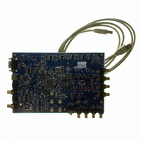
Manufacturer Part Number
CDB42L55
Description
Eval Bd Ultra Low Power Stereo Codec
Manufacturer
Cirrus Logic Inc
Specifications of CDB42L55
Main Purpose
Audio, CODEC
Embedded
Yes, FPGA / CPLD
Utilized Ic / Part
CS42L55
Primary Attributes
2 Stereo Analog Inputs, Stereo Line and Headphone Outputs, S/PDIF Transmitter and Receiver
Secondary Attributes
GUI, USB, RS232, I2C Interfaces, USB or External or Battery Power Supply
Product
Audio Modules
Lead Free Status / RoHS Status
Contains lead / RoHS non-compliant
Lead Free Status / RoHS Status
Contains lead / RoHS non-compliant
Other names
598-1506
CDB-42L55
CDB-42L55


DS773F1
4.11
After the PDN bit is released and MCLK is valid, the quiescent voltage, VQ, and the internal voltage refer-
ence, FILT+, will begin powering up to normal operation. The charge pump slowly powers up and charges
the capacitors. Power is then applied to the headphone amplifiers and switched-capacitor filters, and the an-
alog/digital outputs enter a muted state. MCLK occurrences are counted over one LRCK period to determine
a valid MCLK/LRCK ratio and normal operation begins.
Recommended DAC to HP or Line Power-Up Sequence (Playback)
1. Hold RESET low until the power supplies are stable; no specific power supply sequencing is required.
2. Apply MCLK (LRCK, SCLK and SDIN may be applied at any time) at the appropriate frequency.
3. Bring RESET high.
4. Wait a minimum of 500 ns before writing to the control port.
5. The default state of the master power down bit, PDN, is ‘1’b. Load the following register settings while
6. Load the required register settings detailed in
7. Configure the headphone and line power down controls for ON, OFF, or HPDETECT operation.
8. Configure the serial port I/O control for master or slave operation.
9. Configure the master clock (MCLK) and bit clock (SCLK) I/O control as desired. Refer to
10. Configure the sample rate (LRCK) controls for the desired sample rate. Refer to
11. The default state of the DSP engine’s power down bit, PDN_DSP, is ‘0’b. It is not necessary to power
12. To minimize pops on the headphone or line amplifier, each respective analog volume control must first
13. After muting the headphone or line amplifiers, set the PDN bit to ‘0’b.
14. Wait 75 ms for the headphone or line amplifier to power up.
15. Un-mute and ramp the volume for the headphone or line amplifiers to the desired level.
16. Bring RESET low if the analog or digital supplies drop below the recommended operating condition to
Power Up Sequence
Step 5,
Step
Steps
Step
Step
Step 12a,15a .......................
Step 12b,15b .......................
RESET should be held low for a minimum of 1 ms after power supplies are stable.
keeping the PDN bit set to ‘1’b.
Register Controls: PDN_HPx[1:0], PDN_LINx[1:0]
Register Controls: M/S
Clocking” on page 34
Register Controls: MCLKDIV2, SCK=MCK
ing” on page 34
Register Controls: See Register 05h
down the DSP before changing the various DSP functions. The DSP may be powered down for addi-
tional power savings.
be muted and set to maximum attenuation.
Register Controls: HPxMUTE, LINExMUTE, HPxVOL[6:0], LINExVOL[6:0]
prevent power glitch related issues.
7
10
11
8-9
..................................
13
................................
................................
.............................
............................
for the required configuration for a given sample rate.
Register Location
“Power Down” on page 42
“Power Control 2 (Address 03h)” on page 43
“Clocking Control 1 (Address 04h)” on page 43
“Clocking Control 2 (Address 05h)” on page 44
“Power Down DSP” on page 50
“Headphone Channel x Mute” on page
“Headphone Volume Control” on page
for the required configuration for a given master clock.
4.13 “Required Initialization Settings” on page
57,
57,
“Line Volume Control” on page 58
“Line Channel x Mute” on page 58
4.8 “Serial Port Clock-
4.8 “Serial Port
CS42L55
37.
35
Related parts for CDB42L55
Image
Part Number
Description
Manufacturer
Datasheet
Request
R

Part Number:
Description:
Development Kit
Manufacturer:
Cirrus Logic Inc
Datasheet:
Part Number:
Description:
Development Kit
Manufacturer:
Cirrus Logic Inc
Datasheet:


Part Number:
Description:
High-efficiency PFC + Fluorescent Lamp Driver Reference Design
Manufacturer:
Cirrus Logic Inc
Datasheet:
Part Number:
Description:
Development Kit
Manufacturer:
Cirrus Logic Inc
Datasheet:
Part Number:
Description:
Development Kit
Manufacturer:
Cirrus Logic Inc
Datasheet:

Part Number:
Description:
Development Kit
Manufacturer:
Cirrus Logic Inc
Datasheet:
Part Number:
Description:
Development Kit
Manufacturer:
Cirrus Logic Inc
Datasheet:
Part Number:
Description:
Development Kit
Manufacturer:
Cirrus Logic Inc
Datasheet:
Part Number:
Description:
Development Kit
Manufacturer:
Cirrus Logic Inc
Datasheet:

Part Number:
Description:
EVALUATION BOARD FOR CS8427
Manufacturer:
Cirrus Logic Inc
Datasheet:

Part Number:
Description:
BOARD EVAL FOR CS8416 RCVR
Manufacturer:
Cirrus Logic Inc
Datasheet:

Part Number:
Description:
EVALUATION BOARD FOR CS8420
Manufacturer:
Cirrus Logic Inc
Datasheet:

Part Number:
Description:
KIT DEVELOPMENT EP9315 ARM9
Manufacturer:
Cirrus Logic Inc
Datasheet:

Part Number:
Description:
KIT DEVELOPMENT EP9302 ARM9
Manufacturer:
Cirrus Logic Inc
Datasheet: