CDB42L55 Cirrus Logic Inc, CDB42L55 Datasheet - Page 37
CDB42L55
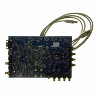
Manufacturer Part Number
CDB42L55
Description
Eval Bd Ultra Low Power Stereo Codec
Manufacturer
Cirrus Logic Inc
Specifications of CDB42L55
Main Purpose
Audio, CODEC
Embedded
Yes, FPGA / CPLD
Utilized Ic / Part
CS42L55
Primary Attributes
2 Stereo Analog Inputs, Stereo Line and Headphone Outputs, S/PDIF Transmitter and Receiver
Secondary Attributes
GUI, USB, RS232, I2C Interfaces, USB or External or Battery Power Supply
Product
Audio Modules
Lead Free Status / RoHS Status
Contains lead / RoHS non-compliant
Lead Free Status / RoHS Status
Contains lead / RoHS non-compliant
Other names
598-1506
CDB-42L55
CDB-42L55


DS773F1
4.13
1. Write 0x99 to register 0x00.
2. Write 0x30 to register 0x2E.
3. Write 0x07 to register 0x32.
4. Write 0xFF to register 0x33.
5. Write 0xF8 to register 0x34.
6. Write 0xDC to register 0x35.
7. Write 0xFC to register 0x36.
8. Write 0xAC to register 0x37.
9. Write 0xF8 to register 0x3A.
10. Write 0xD3 to register 0x3C.
11. Write 0x23 to register 0x3D.
12. Write 0x81 to register 0x3E.
13. Write 0x46 to register 0x3F.
14. Write 0x00 to register 0x00.
Required Initialization Settings
The current required for various sections in the CODEC must be reduced using the control port compensa-
tion strategy shown below. All performance and power consumption measurements were taken with the
Control Port Compensation shown below.
3. Set bit 5 in register 07h to ‘1’b. This implements a high impedance state on the serial output ports to
4. Configure the serial port I/O control for master operation.
5. Power up either one of the ADC channels.
6. Wait 100 ms.
7. Set the PDN bit to ‘1’b. The CODEC is completely powered down in a low power state.
8. To achieve the lowest operating quiescent current, bring RESET low. All control port registers will be
signal. The zero cross timeout, however, is dependent on the serial port clock domain. Thus, to fully
power down, the ADC must briefly power up to enable the zero cross state machine. Follow the
remaining steps below to complete the power down sequence.
avoid possible contention in step
Register Controls: M/S
Register Controls: PDN_ADCx
reset to their default state.
Power Down Sequence
Step 1a ................................
Step 1b ................................
Step
Step
Step
Step
VA < 2.1 V
3
4
5
7
..................................
..................................
..................................
..................................
Register Location
“Headphone Volume Control” on page
“Headphone Channel x Mute” on page
“Miscellaneous Control (Address 07h)” on page 45
“Master/Slave Mode” on page 43
“Power Down ADC x” on page 42
“Power Down” on page 42
1. Write 0x99 to register 0x00.
2. Write 0x30 to register 0x2E.
3. Write 0x07 to register 0x32.
4. Write 0xFD to register 0x33.
5. Write 0xF8 to register 0x34.
6. Write 0xDC to register 0x35.
7. Write 0xF8 to register 0x36.
8. Write 0x6C to register 0x37.
9. Write 0xF8 to register 0x3A.
10. Write 0xD3 to register 0x3C.
11. Write 0x23 to register 0x3D.
12. Write 0x81 to register 0x3E.
13. Write 0x46 to register 0x3F.
14. Write 0x00 to register 0x00.
4
if clocks are already applied to the serial port.
VA > 2.1 V
57,
57,
“Line Volume Control” on page 58
“Line Channel x Mute” on page 58
1. [Enable test register access.]
2. Digital Regulator.
3. ADC.
4. ADC.
5. ADC.
6. Zero Cross Detector.
7. PGA.
8. PGA.
9. DAC.
10. Headphone Amplifier.
11. Headphone & Line Amplifier.
12. Line Amplifier.
13. PGA & ADC.
14. [Disable test register access.].
Current adjustments are made in
the following sections:
CS42L55
37
Related parts for CDB42L55
Image
Part Number
Description
Manufacturer
Datasheet
Request
R

Part Number:
Description:
Development Kit
Manufacturer:
Cirrus Logic Inc
Datasheet:
Part Number:
Description:
Development Kit
Manufacturer:
Cirrus Logic Inc
Datasheet:


Part Number:
Description:
High-efficiency PFC + Fluorescent Lamp Driver Reference Design
Manufacturer:
Cirrus Logic Inc
Datasheet:
Part Number:
Description:
Development Kit
Manufacturer:
Cirrus Logic Inc
Datasheet:
Part Number:
Description:
Development Kit
Manufacturer:
Cirrus Logic Inc
Datasheet:

Part Number:
Description:
Development Kit
Manufacturer:
Cirrus Logic Inc
Datasheet:
Part Number:
Description:
Development Kit
Manufacturer:
Cirrus Logic Inc
Datasheet:
Part Number:
Description:
Development Kit
Manufacturer:
Cirrus Logic Inc
Datasheet:
Part Number:
Description:
Development Kit
Manufacturer:
Cirrus Logic Inc
Datasheet:

Part Number:
Description:
EVALUATION BOARD FOR CS8427
Manufacturer:
Cirrus Logic Inc
Datasheet:

Part Number:
Description:
BOARD EVAL FOR CS8416 RCVR
Manufacturer:
Cirrus Logic Inc
Datasheet:

Part Number:
Description:
EVALUATION BOARD FOR CS8420
Manufacturer:
Cirrus Logic Inc
Datasheet:

Part Number:
Description:
KIT DEVELOPMENT EP9315 ARM9
Manufacturer:
Cirrus Logic Inc
Datasheet:

Part Number:
Description:
KIT DEVELOPMENT EP9302 ARM9
Manufacturer:
Cirrus Logic Inc
Datasheet: