CDB42L55 Cirrus Logic Inc, CDB42L55 Datasheet - Page 4
CDB42L55
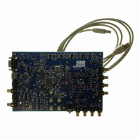
Manufacturer Part Number
CDB42L55
Description
Eval Bd Ultra Low Power Stereo Codec
Manufacturer
Cirrus Logic Inc
Specifications of CDB42L55
Main Purpose
Audio, CODEC
Embedded
Yes, FPGA / CPLD
Utilized Ic / Part
CS42L55
Primary Attributes
2 Stereo Analog Inputs, Stereo Line and Headphone Outputs, S/PDIF Transmitter and Receiver
Secondary Attributes
GUI, USB, RS232, I2C Interfaces, USB or External or Battery Power Supply
Product
Audio Modules
Lead Free Status / RoHS Status
Contains lead / RoHS non-compliant
Lead Free Status / RoHS Status
Contains lead / RoHS non-compliant
Other names
598-1506
CDB-42L55
CDB-42L55


4
5. REGISTER QUICK REFERENCE ........................................................................................................ 40
6. REGISTER DESCRIPTION .................................................................................................................. 42
6.1 Fab I.D. and Revision Register (Address 01h) (Read Only) ........................................................... 42
6.2 Power Control 1 (Address 02h) ...................................................................................................... 42
6.3 Power Control 2 (Address 03h) ...................................................................................................... 43
6.4 Clocking Control 1 (Address 04h) ................................................................................................... 43
6.5 Clocking Control 2 (Address 05h) ................................................................................................... 44
6.6 Class H Power Control (Address 06h) ............................................................................................ 45
6.7 Miscellaneous Control (Address 07h) ............................................................................................. 45
6.8 ADC, Line, HP MUX (Address 08h) ................................................................................................ 46
6.9 HPF Control (Address 09h) ............................................................................................................ 47
6.10 Misc. ADC Control (Address 0Ah) ................................................................................................ 48
6.11 PGA x MUX, Volume:
PGA A (Address 0Bh) & PGA B (Address 0Ch) ................................................................................... 49
6.12 ADCx Attenuator Control:
ADCAATT (Address 0Dh) & ADCBATT (Address 0Eh) ....................................................................... 50
6.13 Playback Control 1 (Address 0Fh) ................................................................................................ 50
6.1.1 Chip Revision (Read Only) .................................................................................................... 42
6.2.1 Power Down ADC Charge Pump .......................................................................................... 42
6.2.2 Power Down ADC x ............................................................................................................... 42
6.2.3 Power Down .......................................................................................................................... 42
6.3.1 Headphone Power Control .................................................................................................... 43
6.3.2 Line Power Control ................................................................................................................ 43
6.4.1 Master/Slave Mode ............................................................................................................... 43
6.4.2 SCLK Polarity ........................................................................................................................ 43
6.4.3 SCLK Equals MCLK .............................................................................................................. 44
6.4.4 MCLK Divide By 2 ................................................................................................................. 44
6.4.5 MCLK Disable ....................................................................................................................... 44
6.5.1 Speed Mode .......................................................................................................................... 44
6.5.2 32 kHz Sample Rate Group .................................................................................................. 45
6.5.3 Internal MCLK/LRCK Ratio ................................................................................................... 45
6.6.1 Adaptive Power Adjustment .................................................................................................. 45
6.7.1 Digital MUX ........................................................................................................................... 45
6.7.2 Analog Zero Cross ................................................................................................................ 46
6.7.3 Digital Soft Ramp .................................................................................................................. 46
6.7.4 Freeze Registers ................................................................................................................... 46
6.8.1 ADC x Input Select ................................................................................................................ 46
6.8.2 Line Input Select .................................................................................................................... 47
6.8.3 Headphone Input Select ........................................................................................................ 47
6.9.1 ADCx High-Pass Filter .......................................................................................................... 47
6.9.2 ADCx High-Pass Filter Freeze .............................................................................................. 47
6.9.3 HPF x Corner Frequency ...................................................................................................... 47
6.10.1 ADC Channel B=A .............................................................................................................. 48
6.10.2 PGA Channel B=A .............................................................................................................. 48
6.10.3 Digital Sum .......................................................................................................................... 48
6.10.4 Invert ADC Signal Polarity ................................................................................................... 48
6.10.5 ADC Mute ............................................................................................................................ 48
6.11.1 Boostx ................................................................................................................................. 49
6.11.2 PGA x Input Select .............................................................................................................. 49
6.11.3 PGAx Volume ...................................................................................................................... 49
6.12.1 ADCx Volume ...................................................................................................................... 50
6.13.1 Power Down DSP ................................................................................................................ 50
6.13.2 HP/Line De-Emphasis ......................................................................................................... 50
6.13.3 Playback Channels B=A ...................................................................................................... 50
CS42L55
DS773F1
Related parts for CDB42L55
Image
Part Number
Description
Manufacturer
Datasheet
Request
R

Part Number:
Description:
Development Kit
Manufacturer:
Cirrus Logic Inc
Datasheet:
Part Number:
Description:
Development Kit
Manufacturer:
Cirrus Logic Inc
Datasheet:


Part Number:
Description:
High-efficiency PFC + Fluorescent Lamp Driver Reference Design
Manufacturer:
Cirrus Logic Inc
Datasheet:
Part Number:
Description:
Development Kit
Manufacturer:
Cirrus Logic Inc
Datasheet:
Part Number:
Description:
Development Kit
Manufacturer:
Cirrus Logic Inc
Datasheet:

Part Number:
Description:
Development Kit
Manufacturer:
Cirrus Logic Inc
Datasheet:
Part Number:
Description:
Development Kit
Manufacturer:
Cirrus Logic Inc
Datasheet:
Part Number:
Description:
Development Kit
Manufacturer:
Cirrus Logic Inc
Datasheet:
Part Number:
Description:
Development Kit
Manufacturer:
Cirrus Logic Inc
Datasheet:

Part Number:
Description:
EVALUATION BOARD FOR CS8427
Manufacturer:
Cirrus Logic Inc
Datasheet:

Part Number:
Description:
BOARD EVAL FOR CS8416 RCVR
Manufacturer:
Cirrus Logic Inc
Datasheet:

Part Number:
Description:
EVALUATION BOARD FOR CS8420
Manufacturer:
Cirrus Logic Inc
Datasheet:

Part Number:
Description:
KIT DEVELOPMENT EP9315 ARM9
Manufacturer:
Cirrus Logic Inc
Datasheet:

Part Number:
Description:
KIT DEVELOPMENT EP9302 ARM9
Manufacturer:
Cirrus Logic Inc
Datasheet: