CDB42L55 Cirrus Logic Inc, CDB42L55 Datasheet - Page 38
CDB42L55
Manufacturer Part Number
CDB42L55
Description
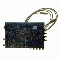
Eval Bd Ultra Low Power Stereo Codec
Manufacturer
Cirrus Logic Inc
Specifications of CDB42L55
Main Purpose
Audio, CODEC
Embedded
Yes, FPGA / CPLD
Utilized Ic / Part
CS42L55
Primary Attributes
2 Stereo Analog Inputs, Stereo Line and Headphone Outputs, S/PDIF Transmitter and Receiver
Secondary Attributes
GUI, USB, RS232, I2C Interfaces, USB or External or Battery Power Supply
Product
Audio Modules
Lead Free Status / RoHS Status
Contains lead / RoHS non-compliant
Lead Free Status / RoHS Status
Contains lead / RoHS non-compliant
Other names
598-1506
CDB-42L55
CDB-42L55


38
4.14
4.14.1 I²C Control
SCL
SDA
SDA
SCL
START
Control Port Operation
The control port is used to access the registers allowing the CODEC to be configured for the desired oper-
ational modes and formats. The operation of the control port may be completely asynchronous with respect
to the audio sample rates. However, to avoid potential interference problems, the control port pins should
remain static if no operation is required.
The control port operates using an I²C interface with the CODEC acting as a slave device.
START
SDA is a bidirectional data line. Data is clocked into and out of the part by the clock, SCL. The signal tim-
ings for a read and write cycle are shown in
falling transition of SDA while the clock is high. A Stop condition is defined as a rising transition of SDA
while the clock is high. All other transitions of SDA occur while the clock is low. The first byte sent to the
CS42L55 after a Start condition consists of a 7-bit chip address field and a R/W bit (high for a read, low
for a write).
The upper 7 bits of the address field are fixed at 1001010. To communicate with the CS42L55, the chip
address field, which is the first byte sent to the CS42L55, should match 1001010. The eighth bit of the
address is the R/W bit. If the operation is a write, the next byte is the Memory Address Pointer (MAP); the
MAP selects the register to be read or written. If the operation is a read, the contents of the register pointed
to by the MAP will be output. Setting the auto-increment bit in MAP allows successive reads or writes of
consecutive registers. Each byte is separated by an acknowledge bit. The ACK bit is output from the
CS42L55 after each input byte is read and is input to the CS42L55 from the microcontroller after each
transmitted byte.
Since the read operation cannot set the MAP, an aborted write operation is used as a preamble. As shown
in
condition. The following pseudocode illustrates an aborted write operation followed by a read operation.
Send start condition.
Send 10010100 (chip address & write operation).
Receive acknowledge bit.
Send MAP byte, auto-increment off.
0
CHIP ADDRESS (WRITE)
Figure
1
0
1
1
CHIP ADDRESS (WRITE)
0
2
1
0
0
3
0
22, the write operation is aborted (after the acknowledge for the MAP byte) by sending a stop
2
1
4
1
0 1 0 0
3
5
0
4
6
1
5
7
0
ACK
6
8
0
9
INCR
7
Figure 22. Control Port Timing, I²C Read
Figure 21. Control Port Timing, I²C Write
10 11
ACK
6
8
INCR
5
9
MAP BYTE
12 13 14 15
4
10 11
6
3
MAP BYTE
5
2
12
4
1
13 14 15
16
3
0
ACK
STOP
2
17 18
START
Figure 21
1
16 17 18
0
19
ACK
1
20 21 22 23 24
CHIP ADDRESS (READ)
0
7
and
0
19
6
DATA
1
Figure
0
24 25
1
1 0 1
0
25
ACK
26 27 28
22. A Start condition is defined as a
26
ACK
27 28
7
7
DATA +1
DATA
6
0
ACK
1
0
DATA +1
7
7
0
DATA +n
6
DATA + n
7
CS42L55
1
0
0
DS773F1
ACK
ACK
NO
STOP
STOP
Related parts for CDB42L55
Image
Part Number
Description
Manufacturer
Datasheet
Request
R

Part Number:
Description:
Development Kit
Manufacturer:
Cirrus Logic Inc
Datasheet:
Part Number:
Description:
Development Kit
Manufacturer:
Cirrus Logic Inc
Datasheet:


Part Number:
Description:
High-efficiency PFC + Fluorescent Lamp Driver Reference Design
Manufacturer:
Cirrus Logic Inc
Datasheet:
Part Number:
Description:
Development Kit
Manufacturer:
Cirrus Logic Inc
Datasheet:
Part Number:
Description:
Development Kit
Manufacturer:
Cirrus Logic Inc
Datasheet:

Part Number:
Description:
Development Kit
Manufacturer:
Cirrus Logic Inc
Datasheet:
Part Number:
Description:
Development Kit
Manufacturer:
Cirrus Logic Inc
Datasheet:
Part Number:
Description:
Development Kit
Manufacturer:
Cirrus Logic Inc
Datasheet:
Part Number:
Description:
Development Kit
Manufacturer:
Cirrus Logic Inc
Datasheet:

Part Number:
Description:
EVALUATION BOARD FOR CS8427
Manufacturer:
Cirrus Logic Inc
Datasheet:

Part Number:
Description:
BOARD EVAL FOR CS8416 RCVR
Manufacturer:
Cirrus Logic Inc
Datasheet:

Part Number:
Description:
EVALUATION BOARD FOR CS8420
Manufacturer:
Cirrus Logic Inc
Datasheet:

Part Number:
Description:
KIT DEVELOPMENT EP9315 ARM9
Manufacturer:
Cirrus Logic Inc
Datasheet:

Part Number:
Description:
KIT DEVELOPMENT EP9302 ARM9
Manufacturer:
Cirrus Logic Inc
Datasheet: