CDB42L55 Cirrus Logic Inc, CDB42L55 Datasheet - Page 27
CDB42L55
Manufacturer Part Number
CDB42L55
Description
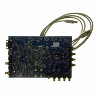
Eval Bd Ultra Low Power Stereo Codec
Manufacturer
Cirrus Logic Inc
Specifications of CDB42L55
Main Purpose
Audio, CODEC
Embedded
Yes, FPGA / CPLD
Utilized Ic / Part
CS42L55
Primary Attributes
2 Stereo Analog Inputs, Stereo Line and Headphone Outputs, S/PDIF Transmitter and Receiver
Secondary Attributes
GUI, USB, RS232, I2C Interfaces, USB or External or Battery Power Supply
Product
Audio Modules
Lead Free Status / RoHS Status
Contains lead / RoHS non-compliant
Lead Free Status / RoHS Status
Contains lead / RoHS non-compliant
Other names
598-1506
CDB-42L55
CDB-42L55


DS773F1
4.5
4.5.1
Class H Amplifier
The CS42L55 headphone and line output amplifiers use a patented Cirrus Logic Bi-Modal Class H technol-
ogy. This technology maximizes operating efficiency of the typical Class AB amplifier while maintaining high
performance. In a Class H amplifier design, the rail voltages supplied to the amplifier vary with the needs of
the music passage that is being amplified. This prevents unnecessarily wasting energy during low power
passages of program material or when the program material is played back at a low volume level.
The central component of the Bi-Modal Class H technology found in the CS42L55 is the internal charge
pump, which creates the rail voltages for the headphone and line amplifiers of the device. The charge pump
receives its input voltage from the voltage present on the VCP pin of the CS42L55. From this input voltage,
the charge pump creates the differential rail voltages that are supplied to the amplifier output stages. The
charge pump is capable of supplying two sets of differential rail voltages. One set is equal to ± VCP and the
other is equal to ± VCP/2.
Referenced Control
Analog Output
ADPTPWR[1:0]
CHGFREQ[3:0]
PDN_HPx[1:0]
PDN_LINx[1:0]
HPxMUTE
HPxVOL[7:0]
LINExMUTE
LINExVOL[7:0]
ANLGZC
PLYBCKB=A
HPxMUX
LINExMUX
Power Control Options
The method by which the CS42L55 decides which set of rail voltages is supplied to the amplifier output
stages depends on the settings of the Adaptive Power bits (ADPTPWR) found in
(Address 06h)” section on page
bits: Mode 00, 01, 10 and 11.
Referenced Control
ADPTPWR[1:0] ...................
from PGAx
from DACx
Register Location
“Adaptive Power Adjustment” on page 45
“Charge Pump Frequency” on page 67
“Headphone Power Control” on page 43
“Line Power Control” on page 43
“Headphone Channel x Mute” on page 57
“Headphone Volume Control” on page 57
“Line Channel x Mute” on page 58
“Line Volume Control” on page 58
“Analog Zero Cross” on page 46
“Playback Channels B=A” on page 50
“Headphone Input Select” on page 47
“Line Input Select” on page 47
VCP
Register Location
“Adaptive Power Adjustment” on page 45
Figure 13. Analog Output Stage
HPxMUX
LINExMUX
45. As detailed in this section, there are four possible settings for these
CHGFREQ[3:0]
ADPTPWR[1:0]
+VCP/2
-VCP/2
+VCP
-VCP
Class H Control
HPxVOL[6:0]
HPxMUTE
ANLGZC
PLYBCKB=A
LINExVOL[6:0]
LINExMUTE
ANLGZC
PLYBCKB=A
-HP Supply
+HP Supply
= HP and Line Supply
PDN_HPx[1:0]
PDN_LINx[1:0]
HP Detection
+Line Supply
-Line Supply
HPREF
LINEREF
HPOUTA
HPOUTB
LINEOUTA
LINEOUTB
+VHPFILT
-VHPFILT
HPDETECT
“Class H Power Control
CS42L55
27
Related parts for CDB42L55
Image
Part Number
Description
Manufacturer
Datasheet
Request
R

Part Number:
Description:
Development Kit
Manufacturer:
Cirrus Logic Inc
Datasheet:
Part Number:
Description:
Development Kit
Manufacturer:
Cirrus Logic Inc
Datasheet:


Part Number:
Description:
High-efficiency PFC + Fluorescent Lamp Driver Reference Design
Manufacturer:
Cirrus Logic Inc
Datasheet:
Part Number:
Description:
Development Kit
Manufacturer:
Cirrus Logic Inc
Datasheet:
Part Number:
Description:
Development Kit
Manufacturer:
Cirrus Logic Inc
Datasheet:

Part Number:
Description:
Development Kit
Manufacturer:
Cirrus Logic Inc
Datasheet:
Part Number:
Description:
Development Kit
Manufacturer:
Cirrus Logic Inc
Datasheet:
Part Number:
Description:
Development Kit
Manufacturer:
Cirrus Logic Inc
Datasheet:
Part Number:
Description:
Development Kit
Manufacturer:
Cirrus Logic Inc
Datasheet:

Part Number:
Description:
EVALUATION BOARD FOR CS8427
Manufacturer:
Cirrus Logic Inc
Datasheet:

Part Number:
Description:
BOARD EVAL FOR CS8416 RCVR
Manufacturer:
Cirrus Logic Inc
Datasheet:

Part Number:
Description:
EVALUATION BOARD FOR CS8420
Manufacturer:
Cirrus Logic Inc
Datasheet:

Part Number:
Description:
KIT DEVELOPMENT EP9315 ARM9
Manufacturer:
Cirrus Logic Inc
Datasheet:

Part Number:
Description:
KIT DEVELOPMENT EP9302 ARM9
Manufacturer:
Cirrus Logic Inc
Datasheet: